- 您現在的位置:買賣IC網 > PDF目錄385342 > GS881Z18T-80I (GSI TECHNOLOGY) 8Mb Pipelined and Flow Through Synchronous NBT SRAMs PDF資料下載
參數資料
| 型號: | GS881Z18T-80I |
| 廠商: | GSI TECHNOLOGY |
| 元件分類: | DRAM |
| 英文描述: | 8Mb Pipelined and Flow Through Synchronous NBT SRAMs |
| 中文描述: | 512K X 18 ZBT SRAM, 14 ns, PQFP100 |
| 封裝: | TQFP-100 |
| 文件頁數: | 25/34頁 |
| 文件大小: | 542K |
| 代理商: | GS881Z18T-80I |
第1頁第2頁第3頁第4頁第5頁第6頁第7頁第8頁第9頁第10頁第11頁第12頁第13頁第14頁第15頁第16頁第17頁第18頁第19頁第20頁第21頁第22頁第23頁第24頁當前第25頁第26頁第27頁第28頁第29頁第30頁第31頁第32頁第33頁第34頁
Rev: 1.10 8/2000
Specifications cited are subject to change without notice. For latest documentation see http://www.gsitechnology.com
25/34
1998, Giga Semconductor, Inc.
Preliminary
.
GS881Z18/36T-11/100/80/66
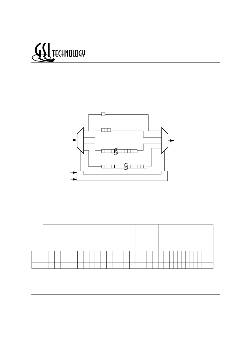
Boundary Scan Register
Boundary Scan Register is a collection of flip flops that can be preset by the logic level found on the RAM’s input or I/O pins. The
flip flops are then daisy chained together so the levels found can be shifted serially out of the JTAG Port’s TDO pin. The Boundary
Scan Register also includes a number of place holder flip flops (always set to a logic 1). The relationship between the device pins
and the bits in the Boundary Scan Register is described in the Scan Order Table following. The Boundary Scan Register, under the
control of the TAP Controller, is loaded with the contents of the RAMs I/O ring when the controller is in Capture-DR state and then
is placed between the TDI and TDO pins when the controller is moved to Shift-DR state. Two TAP instructions can be used to
activate the Boundary Scan Register.
JTAG TAP Block Diagram
Identification (ID) Register
The ID Register is a 32-bit register that is loaded with a device and vendor specific 32-bit code when the controller is put in
Capture-DR state with the IDCODE command loaded in the Instruction Register. The code is loaded from a 32-bit on-chip ROM.
It describes various attributes of the RAM as indicated below. The register is then placed between the TDI and TDO pins when the
controller is moved into Shift-DR state. Bit 0 in the register is the LSB and the first to reach TDO when shifting begins.
ID Register Contents
Tap Controller Instruction Set
Overview
There are two classes of instructions defined in the Standard 1149.1-1990; the standard (Public) instructions, and device specific
Die
Revision
Code
Not Used
I/O
Configuration
GSI Technology
JEDEC Vendor
ID Code
P
Bit #
31 30 29 28 27 26 25 24 23 22 21 20 19 18 17 16 15 14 13 12 11 10 9 8 7 6 5 4 3 2 1
X
X
X
X
0
0
0
0
0
0
0
0
0
0
X
X
X
X
0
0
0
0
0
0
0
0
0
0
0
1
1
x36
0
0
0
0
0
0
0
0
0
1
1
1
0
0
0 0 1 1 0 1 1 0 0 1
0 0 1 1 0 1 1 0 0 1
x18
Instruction Register
ID Code Register
·
31 30 29
Boundary Scan Register
· · ·
· · ·
n
0
1
2
0
1
2
· · ·
0
1
2
· · ·
0
Bypass Register
TDI
TDO
TMS
TCK
Test Access Port (TAP) Controller
相關PDF資料 |
PDF描述 |
|---|---|
| GS881Z36T-100 | 8Mb Pipelined and Flow Through Synchronous NBT SRAMs |
| GS881Z36T-100I | 8Mb Pipelined and Flow Through Synchronous NBT SRAMs |
| GS881Z36T-11 | 8Mb Pipelined and Flow Through Synchronous NBT SRAMs |
| GS881Z36T-11I | 8Mb Pipelined and Flow Through Synchronous NBT SRAMs |
| GS881Z36T-66 | 8Mb Pipelined and Flow Through Synchronous NBT SRAMs |
相關代理商/技術參數 |
參數描述 |
|---|---|
| GS881Z32BD-150 | 制造商:GSI 制造商全稱:GSI Technology 功能描述:9Mb Pipelined and Flow Through Synchronous NBT SRAM |
| GS881Z32BD-150I | 制造商:未知廠家 制造商全稱:未知廠家 功能描述:9Mb Pipelined and Flow Through Synchronous NBT SRAM |
| GS881Z32BD-150IT | 制造商:GSI 制造商全稱:GSI Technology 功能描述:9Mb Pipelined and Flow Through Synchronous NBT SRAM |
| GS881Z32BD-150IV | 制造商:GSI 制造商全稱:GSI Technology 功能描述:9Mb Pipelined and Flow Through Synchronous NBT SRAM |
| GS881Z32BD-150T | 制造商:未知廠家 制造商全稱:未知廠家 功能描述:9Mb Pipelined and Flow Through Synchronous NBT SRAM |
發布緊急采購,3分鐘左右您將得到回復。