- 您現在的位置:買賣IC網 > PDF目錄385353 > HC-5502X (Intersil Corporation) () PDF資料下載
參數資料
| 型號: | HC-5502X |
| 廠商: | Intersil Corporation |
| 英文描述: | () |
| 中文描述: | () |
| 文件頁數: | 13/17頁 |
| 文件大小: | 255K |
| 代理商: | HC-5502X |
4-13
Line Fault Protection
The subscriber loop can exist in a very hostile electrical
environment. It is often in close proximity to very high voltage
power lines, and can be subjected to lightning induced
voltage surges. The SLIC has to provide isolation between
the subscriber loop and the telephone office. Methods for
dealing with longitudinally induced power frequency currents
and excessive DC line current have been discussed.
The most stringent line fault condition that the SLIC has to
withstand is that of the lightning surge.
The Intersil monolithic SLIC in conjunction with a simple low
cost diode bridge can achieve up to 1kV of isolation between
the loop and switch office. The level of isolation is a function
of the packaging technology and geometry together with the
chip layout geometries. One of the principal reasons for
using DI technology for fabricating the SLIC is that it lends
itself most readily to manufacturing monolithic circuits for
high voltage applications.
Figures 8 and 9 show general application circuits for the HC-
5502X and HC-5504X SLICs. A secondary protection diode
bridge is indicated which protects the feed amplifiers during a
fault. Figure 18 illustrates more clearly the fault current paths
during a lightning or transient high voltage strike. Most line
systems will have primary protection networks. They often
take the form of a carbon block or arc discharge device. These
limit the fault voltage to 500V - 1000V peak before it reaches
the switch line cards. Thus when a transient high voltage fault
has occurred, it will be transmitted as a wave front down the
line. The primary protection network limits the voltage to 500V
to 1000V. The attenuated wave front will continue down the
line towards the SLIC. The feed amplifier outputs appear to
the surge as very low impedance paths to the system battery.
Once the surge reaches the feed resistors, fault current will
flow into or out of the feed amplifier output stages until the
relevant protection diodes switch on. Bench measurements
have indicated peak fault currents of up to 150mA into and out
of the SLIC during the finite turn on time of the diode bridge.
Once the necessary diodes have started to conduct all the
fault current will be handled by them. The geometry of the
SLIC and its package has been designed to withstand the full
rated peak fault voltage at its tip (T) and ring (R) terminals: for
ceramic packages this is 500V peak, and for plastic (or epoxy)
packaged SLICs this is 1000V peak. The circuits are rated
against standard lightning characteristics defined by Figure
19. The ceramic package contains an air gap whereas the
plastic packages contain no void. The dielectric constant of air
is lower than that of the epoxy and it is this which breaks down
at lower voltages than the plastic compound.
If the user wishes to characterize SLIC devices under
simulated high voltage fault conditions on the bench, he
should ensure that the negative battery power supply has
sufficient current capability to source the negative peak fault
current and low series inductance. If this is not the case, then
the battery supply could be pulled more negative and destroy
the SLIC if the total (V
B
+ + V
B
-) voltage across it exceeds
75V.
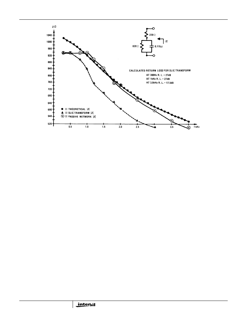
FIGURE 16. |Z| vs FREQUENCY
Application Note 549
相關PDF資料 |
PDF描述 |
|---|---|
| HC-5509A1 | SLIC Subscriber Line Interface Circuit |
| HC4P5509A1-9 | SLIC Subscriber Line Interface Circuit |
| HC4P5509A1-5 | SLIC Subscriber Line Interface Circuit |
| HC1-5509A1-5 | SLIC Subscriber Line Interface Circuit |
| HC3-5509A1-5 | SLIC Subscriber Line Interface Circuit |
相關代理商/技術參數 |
參數描述 |
|---|---|
| HC5503 | 制造商:INTERSIL 制造商全稱:Intersil Corporation 功能描述:Low Cost 24V SLIC For PABX / Key Systems |
| HC5503C | 制造商:INTERSIL 制造商全稱:Intersil Corporation 功能描述:Unbalanced PBX/Key System SLIC, Subscriber Line Interface Circuit |
| HC5503CB | 制造商:Rochester Electronics LLC 功能描述: 制造商:Intersil Corporation 功能描述: |
| HC5503CB96 | 制造商:Rochester Electronics LLC 功能描述:HC5503CB (TAPE&REEL) - Bulk |
| HC5503CBZ | 功能描述:電信線路管理 IC LW COST ISDN SLIC 24S0 RoHS:否 制造商:STMicroelectronics 產品:PHY 接口類型:UART 電源電壓-最大:18 V 電源電壓-最小:8 V 電源電流:30 mA 最大工作溫度:+ 85 C 最小工作溫度:- 40 C 安裝風格:SMD/SMT 封裝 / 箱體:VFQFPN-48 封裝:Tray |
發布緊急采購,3分鐘左右您將得到回復。