- 您現(xiàn)在的位置:買賣IC網(wǎng) > PDF目錄385353 > HC-5502X (Intersil Corporation) () PDF資料下載
參數(shù)資料
| 型號: | HC-5502X |
| 廠商: | Intersil Corporation |
| 英文描述: | () |
| 中文描述: | () |
| 文件頁數(shù): | 5/17頁 |
| 文件大小: | 255K |
| 代理商: | HC-5502X |
4-5
set reference level, the transconductance amplifier sources
current. This current will charge C3 in positive direction causing
the R
F
(Ring Feed) voltage to approach the TF (Tip Feed),
effectively reducing the battery feed across the loop which will
limit the DC loop current. C3 will continue to charge until an
equilibrium level is attained at I
LOOP
= I
LOOP
MAXmA. The
timeconstantofthisfeedbackloopissetbyR21(90k
)andC3
which is nominally 0.33
μ
F.
The R
F
voltage level is also modified to reduce or control
loop current during ring line faults (e.g. ground or power line
crosses), and thermal overload. Figure 2 illustrates this. It
can be seen that the thermal and fault current circuitry works
in parallel with the transconductance amplifier.
Longitudinal Amplifier
The longitudinal amplifier is an op amp configured as a
closed loop differential amplifier with a nominal gain of 0.1
(HC-5504X) or 0.581 (HC-5502X). The output is a measured
of any imbalance between ITIP and IRING as described in
Figure 1. The transfer function of this amplifier is given by:
V
LONG
= K(I
TIP
- I
RING
) 150
Where K is the gain factor of the amplifier. The gain factor is
much less than one since ring voltage (up to 150V
PEAK
) can
appear at the Ring or Ring Feed Sense terminals and are
attenuated to protect the amplifier.
The longitudinal amplifier’s principal functions are Ring Tip
Detection (RTD) and Ground Key Detection (GKD). GKD
provides a means for the subscriber to flag a PBX attendant
and is used extensively in Europe. The ring line is grounded at
the telephone set via a push switch incorporated within the
telephone. This causes a DC current imbalances between the
tip and ring sides of the loop which gives rise to a negative
voltage at the output of the longitudinal amplifier. The output
of the amplifier after being filtered by R20 and C4 to attenuate
AC signals is fed into a detector whose output GK gates the
necessary logic to drive GKD or inhibit the ring relay driver to
remove ringing signals from the line in an off-hook condition.
In order to prevent false ground key owing to line noise or
during ring trip, the internal GKD logic is delayed via C2. An
internal current source of 5
μ
A has to change C2 up to a 5V
level before allowing the ground key signal to propagate.
Thus, for C2 = 0.15
μ
F, a delay of 150ms is established.
Ringing the line and Ring Trip Detection are discussed more
fully in the following section, Designing with the Intersil SLIC.
Uncommitted Op Amp
An uncommitted op amp is provided on the chip. This is a
standard op amp with an output swing of
±
5V. It is primarily
intended to be used to balance the transhybrid return signal
discussed in The Transversal Amplifier (TA) section. The
amplifier has an offset voltage of 10mV; an open loop gain of
66dB; a GBW product of 2MHz; slews at 1V/
μ
s typically, and
has a
±
2mA output current drive capability.
The Logic Network
The logic network utilizes I
2
L logic. All external inputs and
outputs are LS TTL compatible: the relay driver is an open
collector output that can sink 60mA with a V
CE
of 1V.
Figure 7 is a schematic of the combination logic within the
network. The external inputs RC (Relay Control) and PD
(Power Denial) allow the switch controller to ring the line or
deny power to the loop, respectively. The Ring
Synchronization input (RS) facilitates switching of the ring
relay near a ring current zero crossing in order to minimize
inductive kick-back from the telephone ringer.
The internal inputs SH and GK control ring trip and provide
supervisory flags to the system controller via the Switch
Hook Detect (SHD) and Ground Key Detect (GKD) outputs.
Designing with the Intersil SLIC
General application circuits for the HC-5502X and HC-5504X
SLICs are given in Figures 8 and 9. In this section, several
specific design and application areas will be discussed:
Ringing the Line
Power Denial
Transhybrid and Longitudinal Balance
Complex Impedance Matching
Surge Protection
Ringing The Line
The HC-5502X is used for tip injected ringing (also called
single ended ground referenced ringing), and the HC-5504X
is used for ring injected or single ended battery referenced
ringing. Figures 10 and 11 show the two different ringing
schemes. Note, that the HC-5504X can be used for either of
the single ended ringing schemes: to use the HC-5504 for tip
injected ringing the Ring Feed Sense (RFS) and R
F
pins are
permanently connected externally, and the scheme shown in
Figure 10 adopted.
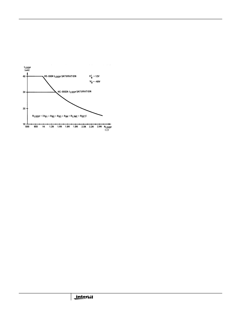
FIGURE 6. DC LOOP CURRENT CHARACTERISTICS
Application Note 549
相關(guān)PDF資料 |
PDF描述 |
|---|---|
| HC-5509A1 | SLIC Subscriber Line Interface Circuit |
| HC4P5509A1-9 | SLIC Subscriber Line Interface Circuit |
| HC4P5509A1-5 | SLIC Subscriber Line Interface Circuit |
| HC1-5509A1-5 | SLIC Subscriber Line Interface Circuit |
| HC3-5509A1-5 | SLIC Subscriber Line Interface Circuit |
相關(guān)代理商/技術(shù)參數(shù) |
參數(shù)描述 |
|---|---|
| HC5503 | 制造商:INTERSIL 制造商全稱:Intersil Corporation 功能描述:Low Cost 24V SLIC For PABX / Key Systems |
| HC5503C | 制造商:INTERSIL 制造商全稱:Intersil Corporation 功能描述:Unbalanced PBX/Key System SLIC, Subscriber Line Interface Circuit |
| HC5503CB | 制造商:Rochester Electronics LLC 功能描述: 制造商:Intersil Corporation 功能描述: |
| HC5503CB96 | 制造商:Rochester Electronics LLC 功能描述:HC5503CB (TAPE&REEL) - Bulk |
| HC5503CBZ | 功能描述:電信線路管理 IC LW COST ISDN SLIC 24S0 RoHS:否 制造商:STMicroelectronics 產(chǎn)品:PHY 接口類型:UART 電源電壓-最大:18 V 電源電壓-最小:8 V 電源電流:30 mA 最大工作溫度:+ 85 C 最小工作溫度:- 40 C 安裝風格:SMD/SMT 封裝 / 箱體:VFQFPN-48 封裝:Tray |
發(fā)布緊急采購,3分鐘左右您將得到回復。