- 您現在的位置:買賣IC網 > PDF目錄385381 > HI7190IP (INTERSIL CORP) null24-Bit, High Precision, Sigma Delta A/D Converter PDF資料下載
參數資料
| 型號: | HI7190IP |
| 廠商: | INTERSIL CORP |
| 元件分類: | ADC |
| 英文描述: | null24-Bit, High Precision, Sigma Delta A/D Converter |
| 中文描述: | 1-CH 24-BIT DELTA-SIGMA ADC, SERIAL ACCESS, PDIP20 |
| 封裝: | PLASTIC, MS-001AD, DIP-20 |
| 文件頁數: | 13/24頁 |
| 文件大小: | 187K |
| 代理商: | HI7190IP |
1883
Conversion Mode
For Conversion Mode operation the HI7190 converts the dif-
ferential voltage between V
INHI
and V
INLO
. From switching
into this mode it takes 3 conversion periods (3 x 1/f
N
) for
DRDY to go low and new data to be valid. No calibration
coefficients are generated when operating in Conversion
Mode as data is calibrated using the existing calibration
coefficients.
Self-Calibration Mode
Please note: Self-calibration is only valid when operating
in a gain of one. In addition, the offset and gain errors are
not reduced as with the full system calibration.
The Self-Calibration Mode is a three step process that
updates the Offset Calibration Register, the Positive Full
Scale Calibration Register, and the Negative Full Scale Cali-
bration Register. In this mode an internal offset calibration is
done by disconnecting the external inputs and shorting the
inputs of the PGIA together. After 3 conversion periods the
Offset Calibration Register is updated with the value that
corrects any internal offset errors.
After the offset calibration is completed the Positive and
Negative Full Scale Calibration Registers are updated. The
inputs V
INHI
and V
INLO
are disconnected and the external
reference is applied across the modulator inputs. The
HI7190 then takes 3 conversion cycles to sample the data
and update the Positive Full Scale Calibration Register. Next
the polarity of the reference voltage across the modulator
input terminals is reversed and after 3 conversion cycles the
Negative Full Scale Calibration Register is updated. The
values stored in the Positive and Negative Full Scale
Calibration Registers correct for any internal gain errors in
the A/D transfer function. After 3 more conversion cycles the
DRDY line will activate signaling that the calibration is com-
plete and valid data is present in the Data Output Register.
System Offset Calibration Mode
The System Offset Calibration Mode is a single step process
that allows the user to lump offset errors of external circuitry
and the internal errors of the HI7190 together and null them
out. This mode will convert the external differential signal
applied to the V
IN
inputs and then store that value in the Off-
set Calibration Register. The user must apply the zero point
or offset voltage to the HI7190 analog inputs and allow the
signal to settle
before
selecting this mode.After 4 conver-
sion periods the DRDY line will activate signaling that the
calibration is complete and valid data is present in the Data
Output Register.
System Positive Full Scale Calibration Mode
The System Positive Full Scale Calibration Mode is a single
step process that allows the user to lump gain errors of
external circuitry and the internal errors of the HI7190
together and null them out. This mode will convert the exter-
nal differential signal applied to the V
IN
inputs and stores the
converted value in the Positive Full Scale Calibration Regis-
ter. The user must apply the +Full Scale voltage to the
HI7190 analog inputs and allow the signal to settle
before
selecting this mode.After 4 conversion periods the DRDY
line will activate signaling the calibration is complete and
valid data is present in the Data Output Register.
System Negative Full Scale Calibration Mode
The System Negative Full Scale Calibration Mode is a
single-step process that allows the user to lump gain errors
of external circuitry and the internal errors of the HI7190
together and null them out. This mode will convert the exter-
nal differential signal applied to the V
IN
inputs and stores the
converted value in the Negative Full Scale Calibration Regis-
ter. The user must apply the -Full Scale voltage to the
HI7190 analog inputs and allow the signal to settle
before
selecting this mode.After 4 conversion periods the DRDY
line will activate signaling the calibration is complete and
valid data is present in the Data Output Register.
System Offset/Internal Gain Calibration Mode
Please note: System Offset/Internal Gain is only valid
when operating in a gain of one. In addition, the offset and
gain errors are not reduced as with the full system calibra-
tion.
The System Offset/Internal Gain Calibration Mode is a single
step process that updates the Offset Calibration Register,
the Positive Full Scale Calibration Register, and the Negative
Full Scale Calibration Register. First the external differential
signal applied to the V
IN
inputs is converted and that value is
stored in the Offset Calibration Register. The user must
apply the zero point or offset voltage to the HI7190 analog
inputs and allow the signal to settle
before
selecting this
mode.
After this is completed the Positive and Negative Full Scale
Calibration Registers are updated. The inputs V
INHI
and V
INLO
are disconnected and the external reference is switched in. The
HI7190 then takes 3 conversion cycles to sample the data and
update the Positive Full Scale Calibration Register. Next the
polarity of the reference voltage across the V
INHI
and V
INLO
terminals is reversed and after 3 conversion cycles the
Negative Full Calibration Register is updated. The values
stored in the Positive and Negative Full Scale Calibration
Registers correct for any internal gain errors in the A/D transfer
function. After 3 more conversion cycles, the DRDY line will
activate signaling that the calibration is complete and valid data
is present in the Data Output Register.
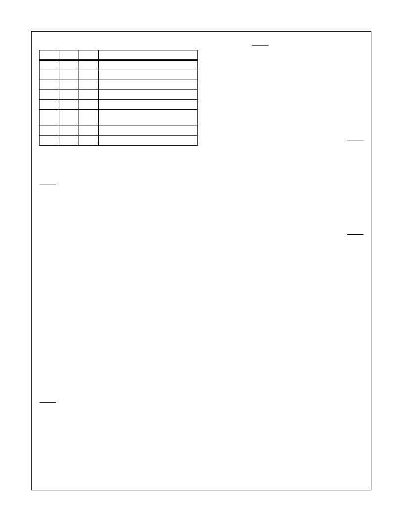
TABLE 4. HI7190 OPERATIONAL MODES
MD2
MD1
MD0
OPERATIONAL MODE
0
0
0
Conversion
0
0
1
Self Calibration (Gain of 1 only)
0
1
0
System Offset Calibration
0
1
1
System Positive Full Scale Calibration
1
0
0
System Negative Full Scale Calibration
1
0
1
System Offset/Internal Gain Calibration
(Gain of 1 only)
1
1
0
System Gain Calibration
1
1
1
Reserved
HI7190
相關PDF資料 |
PDF描述 |
|---|---|
| HI7190EVAL | null24-Bit, High Precision, Sigma Delta A/D Converter |
| HI7190IB | null24-Bit, High Precision, Sigma Delta A/D Converter |
| HIH-3602-A | Humidity Sensor(濕度傳感器) |
| HIH-3602-L-CP | Humidity Sensor(濕度傳感器) |
| HIN240 | 5V High-Speed RS-232 Transceivers with 0.1uF Capacitors |
相關代理商/技術參數 |
參數描述 |
|---|---|
| HI7190IPZ | 功能描述:模數轉換器 - ADC W/ANNEAL ADC 24BIT 1 0HZ SIGMADELTA RoHS:否 制造商:Texas Instruments 通道數量:2 結構:Sigma-Delta 轉換速率:125 SPs to 8 KSPs 分辨率:24 bit 輸入類型:Differential 信噪比:107 dB 接口類型:SPI 工作電源電壓:1.7 V to 3.6 V, 2.7 V to 5.25 V 最大工作溫度:+ 85 C 安裝風格:SMD/SMT 封裝 / 箱體:VQFN-32 |
| HI7191 | 制造商:INTERSIL 制造商全稱:Intersil Corporation 功能描述:24-Bit, High Precision, Sigma Delta A/D Converter |
| HI7191_06 | 制造商:INTERSIL 制造商全稱:Intersil Corporation 功能描述:24-Bit, High Precision, Sigma Delta A/D Converter |
| HI7191IB | 功能描述:IC ADC 24BIT PROGBL SER 20-SOIC RoHS:否 類別:集成電路 (IC) >> 數據采集 - 模數轉換器 系列:- 產品培訓模塊:Lead (SnPb) Finish for COTS Obsolescence Mitigation Program 標準包裝:2,500 系列:- 位數:12 采樣率(每秒):3M 數據接口:- 轉換器數目:- 功率耗散(最大):- 電壓電源:- 工作溫度:- 安裝類型:表面貼裝 封裝/外殼:SOT-23-6 供應商設備封裝:SOT-23-6 包裝:帶卷 (TR) 輸入數目和類型:- |
| HI7191IBZ | 功能描述:模數轉換器 - ADC ADC 24BIT SIGMADELTA 20 IND RoHS:否 制造商:Texas Instruments 通道數量:2 結構:Sigma-Delta 轉換速率:125 SPs to 8 KSPs 分辨率:24 bit 輸入類型:Differential 信噪比:107 dB 接口類型:SPI 工作電源電壓:1.7 V to 3.6 V, 2.7 V to 5.25 V 最大工作溫度:+ 85 C 安裝風格:SMD/SMT 封裝 / 箱體:VQFN-32 |
發布緊急采購,3分鐘左右您將得到回復。