- 您現在的位置:買賣IC網 > PDF目錄385381 > HI7190IP (INTERSIL CORP) null24-Bit, High Precision, Sigma Delta A/D Converter PDF資料下載
參數資料
| 型號: | HI7190IP |
| 廠商: | INTERSIL CORP |
| 元件分類: | ADC |
| 英文描述: | null24-Bit, High Precision, Sigma Delta A/D Converter |
| 中文描述: | 1-CH 24-BIT DELTA-SIGMA ADC, SERIAL ACCESS, PDIP20 |
| 封裝: | PLASTIC, MS-001AD, DIP-20 |
| 文件頁數: | 3/24頁 |
| 文件大小: | 187K |
| 代理商: | HI7190IP |
1873
Absolute Maximum Ratings
Thermal Information
Supply Voltage
AV
DD
to AGND . . . . . . . . . . . . . . . . . . . . . . . . . . . . . . . . . . .+5.5V
AV
SS
to AGND . . . . . . . . . . . . . . . . . . . . . . . . . . . . . . . . . . . -5.5V
DV
DD
to DGND. . . . . . . . . . . . . . . . . . . . . . . . . . . . . . . . . . +5.5V
DGND to AGND . . . . . . . . . . . . . . . . . . . . . . . . . . . . . . . . .
±
0.3V
Analog Input Pins . . . . . . . . . . . . . . . . . . . . . . . . . . . . AV
SS
to AV
DD
Digital Input, Output and I/O Pins. . . . . . . . . . . . . . . DGND to DV
DD
ESD Tolerance (No Damage)
Human Body Model . . . . . . . . . . . . . . . . . . . . . . . . . . . . . . . 500V
Machine Model . . . . . . . . . . . . . . . . . . . . . . . . . . . . . . . . . . +100V
Charged Device Model . . . . . . . . . . . . . . . . . . . . . . . . . . . . 1000V
Operating Conditions
Temperature Range . . . . . . . . . . . . . . . . . . . . . . . . . . -40
o
C to 85
o
C
Thermal Resistance (Typical, Note 1)
PDIP Package . . . . . . . . . . . . . . . . . . . . . . . . . . . . .
SOIC Package. . . . . . . . . . . . . . . . . . . . . . . . . . . . .
Maximum Junction Temperature
Plastic Packages . . . . . . . . . . . . . . . . . . . . . . . . . . . . . . . . . 150
o
C
Maximum Storage Temperature Range . . . . . . . . . .-65
o
C to 150
o
C
Maximum Lead Temperature (Soldering, 10s) . . . . . . . . . . . . 300
o
C
(SOIC - Lead Tips Only)
θ
JA
(
o
C/W)
125
100
CAUTION: Stresses above those listed in “Absolute Maximum Ratings” may cause permanent damage to the device. This is a stress only rating and operation
of the device at these or any other conditions above those indicated in the operational sections of this specification is not implied.
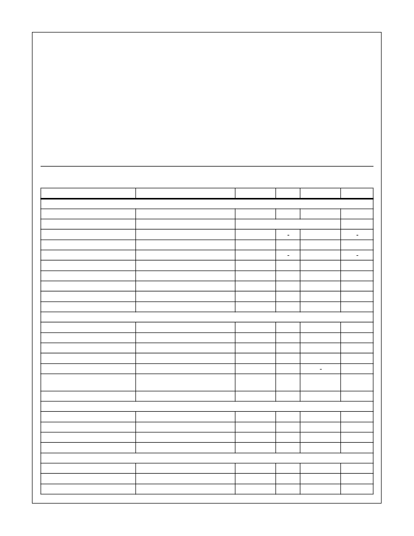
Electrical Specifications
AV
DD
= +5V, AV
SS
= -5V, DV
DD
= +5V, V
RHI
= +2.5V, V
RLO
= AGND = 0V, V
CM
= AGND,
PGIA Gain = 1, OSC
IN
= 10MHz, Bipolar Input Range Selected, f
N
= 10Hz
PARAMETER
TEST CONDITIONS
MIN
TYP
MAX
UNITS
SYSTEM PERFORMANCE
Integral Non-Linearity, INL
End Point Line Method (Notes 3, 5, 6)
-
±
0.0007
±
0.0015
%FS
Differential Non-Linearity
(Note 2)
No Missing codes to 22-Bits
LSB
Offset Error, V
OS
See Table 1
-
-
-
-
Offset Error Drift
V
INHI
= V
INLO
(Notes 3, 8)
-
1
-
μ
V/
o
C
Full Scale Error, FSE
V
INHI
- V
INLO
= +2.5V (Notes 3, 5, 8, 10)
-
-
-
-
Noise, e
N
See Table 1
-
-
-
-
Common Mode Rejection Ratio, CMRR V
CM
= 0V, V
INHI
= V
INLO
from -2V to +2V
-70
-
dB
Normal Mode 50Hz Rejection
Filter Notch = 10Hz, 25Hz, 50Hz (Note 2)
-120
-
-
dB
Normal Mode 60Hz Rejection
Filter Notch = 10Hz, 30Hz, 60Hz (Note 2)
-120
-
-
dB
Step Response Settling Time
-
2
4
Conversions
ANALOG INPUTS
Input Voltage Range
Unipolar Mode (Note 9)
0
-
V
REF
V
Input Voltage Range
Bipolar Mode (Note 9)
- V
REF
-
V
REF
V
Common Mode Input Range
(Note 2)
AV
SS
-
AV
DD
V
Input Leakage Current, I
IN
V
IN
= AV
DD
(Note 2)
-
-
1.0
nA
Input Capacitance, C
IN
-
5.0
-
pF
Reference Voltage Range, V
REF
(V
REF
= V
RHI
- V
RLO
)
2.5
-
5
V
Transducer Burn-Out Current, I
BO
-
200
-
nA
CALIBRATION LIMITS
Positive Full Scale Calibration Limit
-
-
1.2(V
REF
/Gain)
-
Negative Full Scale Calibration Limit
-
-
1.2(V
REF
/Gain)
-
Offset Calibration Limit
-
-
1.2(V
REF
/Gain)
-
Input Span
0.2(V
REF
/Gain)
-
2.4(V
REF
/Gain)
-
DIGITAL INPUTS
Input Logic High Voltage, V
IH
(Note 11)
2.0
-
-
V
Input Logic Low Voltage, V
IL
-
-
0.8
V
Input Logic Current, I
I
V
IN
= 0V, +5V
-
1.0
10
μ
A
HI7190
相關PDF資料 |
PDF描述 |
|---|---|
| HI7190EVAL | null24-Bit, High Precision, Sigma Delta A/D Converter |
| HI7190IB | null24-Bit, High Precision, Sigma Delta A/D Converter |
| HIH-3602-A | Humidity Sensor(濕度傳感器) |
| HIH-3602-L-CP | Humidity Sensor(濕度傳感器) |
| HIN240 | 5V High-Speed RS-232 Transceivers with 0.1uF Capacitors |
相關代理商/技術參數 |
參數描述 |
|---|---|
| HI7190IPZ | 功能描述:模數轉換器 - ADC W/ANNEAL ADC 24BIT 1 0HZ SIGMADELTA RoHS:否 制造商:Texas Instruments 通道數量:2 結構:Sigma-Delta 轉換速率:125 SPs to 8 KSPs 分辨率:24 bit 輸入類型:Differential 信噪比:107 dB 接口類型:SPI 工作電源電壓:1.7 V to 3.6 V, 2.7 V to 5.25 V 最大工作溫度:+ 85 C 安裝風格:SMD/SMT 封裝 / 箱體:VQFN-32 |
| HI7191 | 制造商:INTERSIL 制造商全稱:Intersil Corporation 功能描述:24-Bit, High Precision, Sigma Delta A/D Converter |
| HI7191_06 | 制造商:INTERSIL 制造商全稱:Intersil Corporation 功能描述:24-Bit, High Precision, Sigma Delta A/D Converter |
| HI7191IB | 功能描述:IC ADC 24BIT PROGBL SER 20-SOIC RoHS:否 類別:集成電路 (IC) >> 數據采集 - 模數轉換器 系列:- 產品培訓模塊:Lead (SnPb) Finish for COTS Obsolescence Mitigation Program 標準包裝:2,500 系列:- 位數:12 采樣率(每秒):3M 數據接口:- 轉換器數目:- 功率耗散(最大):- 電壓電源:- 工作溫度:- 安裝類型:表面貼裝 封裝/外殼:SOT-23-6 供應商設備封裝:SOT-23-6 包裝:帶卷 (TR) 輸入數目和類型:- |
| HI7191IBZ | 功能描述:模數轉換器 - ADC ADC 24BIT SIGMADELTA 20 IND RoHS:否 制造商:Texas Instruments 通道數量:2 結構:Sigma-Delta 轉換速率:125 SPs to 8 KSPs 分辨率:24 bit 輸入類型:Differential 信噪比:107 dB 接口類型:SPI 工作電源電壓:1.7 V to 3.6 V, 2.7 V to 5.25 V 最大工作溫度:+ 85 C 安裝風格:SMD/SMT 封裝 / 箱體:VQFN-32 |
發布緊急采購,3分鐘左右您將得到回復。