- 您現在的位置:買賣IC網 > PDF目錄385414 > HY27USxxx (Hynix Semiconductor Inc.) 512Mbit (64Mx8bit / 32Mx16bit) NAND Flash PDF資料下載
參數資料
| 型號: | HY27USxxx |
| 廠商: | Hynix Semiconductor Inc. |
| 英文描述: | 512Mbit (64Mx8bit / 32Mx16bit) NAND Flash |
| 中文描述: | 512兆(64Mx8bit / 32Mx16bit)NAND閃存 |
| 文件頁數: | 17/43頁 |
| 文件大小: | 729K |
| 代理商: | HY27USXXX |
第1頁第2頁第3頁第4頁第5頁第6頁第7頁第8頁第9頁第10頁第11頁第12頁第13頁第14頁第15頁第16頁當前第17頁第18頁第19頁第20頁第21頁第22頁第23頁第24頁第25頁第26頁第27頁第28頁第29頁第30頁第31頁第32頁第33頁第34頁第35頁第36頁第37頁第38頁第39頁第40頁第41頁第42頁第43頁
Rev 0.6 / Oct. 2004
17
HY27SS(08/16)121M Series
HY27US(08/16)121M Series
512Mbit (64Mx8bit / 32Mx16bit) NAND Flash
Page Program
The Page Program operation is the standard operation to program data to the memory array. The main area of the
memory array is programmed by page, however partial page programming is allowed where any number of bytes (1 to
528) or words (1 to 264) can be programmed.
The max number of consecutive partial page program operations allowed in the same page is one in the main area and
two in the spare area. After exceeding this a Block Erase command must be issued before any further program opera-
tions can take place in that page.
Before starting a Page Program operation a Pointer operation can be performed to point to the area to be pro-
grammed. Refer to the Pointer Operations section and Figure 9 for details.
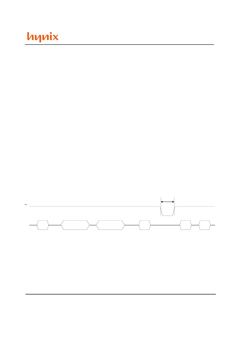
Each Page Program operation consists of five steps (see Figure 14):
1. one bus cycle is required to setup the Page Program command
2. four bus cycles are then required to input the program address (refer to Table 3)
3. the data is then input (up to 528 Bytes/ 264 Words) and loaded into the Page Buffer
4. one bus cycle is required to issue the confirm command to start the Program/ Erase/Read Controller.
5. The Program/ Erase/Read Controller then programs the data into the array.
Once the program operation has started the Status Register can be read using the Read Status Register command.
During program operations the Status Register will only flag errors for bits set to '1' that have not been successfully
programmed to '0'.
During the program operation, only the Read Status Register and Reset commands will be accepted, all other com-
mands will be ignored.
Once the program operation has completed the Program/ Erase/Read Controller bit SR6 is set to '1' and the Ready/
Busy signal goes High.
The device remains in Read Status Register mode until another valid command is written to the Command Interface.
Note: Before starting a Page Program operation a Pointer operation can be performed. Refer to Pointer section for details.
Figure 14. Page Program Operation
Address Inputs
I/O
80h
Page Program
Setup Code
Data Input
10h
70h
SR0
Confirm
Code
Read Status Register
Busy
tBLBH2
(Program Busy time)
RB
相關PDF資料 |
PDF描述 |
|---|---|
| HY27US16121M | 512Mbit (64Mx8bit / 32Mx16bit) NAND Flash |
| HY29F002TC-70 | 2 Megabit (256K x 8), 5 Volt-only, Flash Memory |
| HY29F002TC-45 | 2 Megabit (256K x 8), 5 Volt-only, Flash Memory |
| HY29F002TC-55 | 2 Megabit (256K x 8), 5 Volt-only, Flash Memory |
| HY29F002T | 2 Megabit (256K x 8), 5 Volt-only, Flash Memory |
相關代理商/技術參數 |
參數描述 |
|---|---|
| HY29DL162 | 制造商:未知廠家 制造商全稱:未知廠家 功能描述:16M(X8/X16)|3.0V DUAL BANK|70|NOR FLASH - 16M |
| HY29DL162BF-12 | 制造商:HYNIX 制造商全稱:Hynix Semiconductor 功能描述:16 Megabit (2M x 8/1M x16) Low Voltage, Dual Bank, Simultaneous Read/Write Flash Memory |
| HY29DL162BF-12I | 制造商:HYNIX 制造商全稱:Hynix Semiconductor 功能描述:16 Megabit (2M x 8/1M x16) Low Voltage, Dual Bank, Simultaneous Read/Write Flash Memory |
| HY29DL162BF-70 | 制造商:HYNIX 制造商全稱:Hynix Semiconductor 功能描述:16 Megabit (2M x 8/1M x16) Low Voltage, Dual Bank, Simultaneous Read/Write Flash Memory |
| HY29DL162BF-70I | 制造商:HYNIX 制造商全稱:Hynix Semiconductor 功能描述:16 Megabit (2M x 8/1M x16) Low Voltage, Dual Bank, Simultaneous Read/Write Flash Memory |
發布緊急采購,3分鐘左右您將得到回復。