- 您現(xiàn)在的位置:買賣IC網 > PDF目錄385414 > HY29F002TC-45 (HYNIX SEMICONDUCTOR INC) 2 Megabit (256K x 8), 5 Volt-only, Flash Memory PDF資料下載
參數(shù)資料
| 型號: | HY29F002TC-45 |
| 廠商: | HYNIX SEMICONDUCTOR INC |
| 元件分類: | DRAM |
| 英文描述: | 2 Megabit (256K x 8), 5 Volt-only, Flash Memory |
| 中文描述: | 256K X 8 FLASH 5V PROM, 45 ns, PQCC32 |
| 封裝: | PLASTIC, LCC-32 |
| 文件頁數(shù): | 15/38頁 |
| 文件大小: | 381K |
| 代理商: | HY29F002TC-45 |
第1頁第2頁第3頁第4頁第5頁第6頁第7頁第8頁第9頁第10頁第11頁第12頁第13頁第14頁當前第15頁第16頁第17頁第18頁第19頁第20頁第21頁第22頁第23頁第24頁第25頁第26頁第27頁第28頁第29頁第30頁第31頁第32頁第33頁第34頁第35頁第36頁第37頁第38頁
15
Rev. 4.1/May 01
HY29F002T
WRITE OPERATION STATUS
The HY29F002T provides a number of facilities to
determine the status of a program or erase op-
eration. These are provided through certain bits
of a status word which can be read from the de-
vice during the programming and erase operations.
Table 6 summarizes the status indications and
further detail is provided in the subsections which
follow.
DQ[7] - Data# Polling
The Data# (
“
Data Bar
”
) Polling bit, DQ[7], indicates
to the host system whether an Automatic Algo-
rithm is in progress or completed, or whether the
device is in Erase Suspend mode. Data# Polling
is valid after the rising edge of the final WE# pulse
in the Program or Erase command sequence.
The system must do a read at the program ad-
dress to obtain valid programming status informa-
tion on this bit. While a programming operation is
in progress, the device outputs the complement
of the value programmed to DQ[7]. When the pro-
gramming operation is complete, the device out-
puts the value programmed to DQ[7]. If a pro-
gram operation is attempted within a protected
sector, Data# Polling on DQ[7] is active for ap-
proximately 2 μs, then the device returns to read-
ing array data.
The host must read at an address within any non-
protected sector scheduled for erasure to obtain
valid erase status information on DQ[7]. During
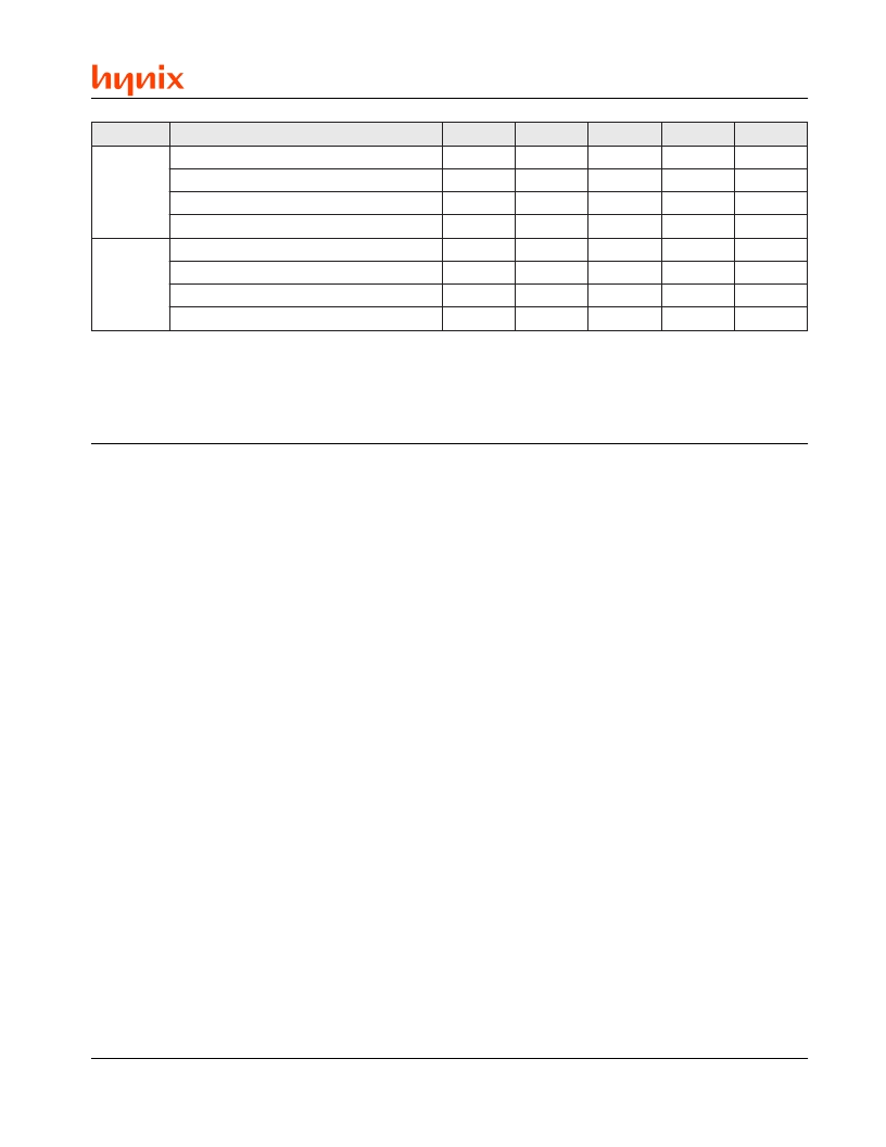
Table 6. Write and Erase Operation Status Summary
e
d
o
M
p
O
o
r
n
g
n
m
m
a
r
o
r
P
e
m
o
c
g
n
m
m
a
r
o
r
P
s
s
e
r
o
r
n
e
s
a
r
E
d
e
m
o
c
e
s
a
r
E
e
s
a
r
n
w
d
a
e
R
r
-
o
n
n
w
d
a
e
R
o
r
n
g
n
m
m
a
r
o
r
P
e
m
o
c
g
n
m
m
a
r
o
r
P
Notes:
1. A valid address is required when reading status information. See text for additional information.
2. DQ[5] status switches to a
‘
1
’
when a program or erase operation exceeds the maximum timing limit.
3. A
‘
1
’
during sector erase indicates that the 50 μs timeout has expired and active erasure is in progress. DQ[3] is not
applicable to the chip erase operation.
4. Equivalent to
‘
No Toggle
’
because data is obtained in this state.
5. Programming can be done only in a non-suspended sector (a sector not marked for erasure).
n
o
r
e
e
r
]
[
#
Q
D
a
D
0
1
1
a
D
#
Q
D
a
D
Q
D
1
]
[
e
g
o
T
a
D
e
g
o
T
a
D
o
o
N
a
D
g
o
T
a
D
Q
D
]
[
Q
D
1
a
D
1
a
D
0
a
D
1
a
D
]
[
A
Q
N
a
D
1
3
a
D
/
N
a
D
/
N
a
D
D
]
[
A
/
a
D
e
g
o
T
a
D
e
g
o
T
a
D
/
N
a
D
Q
N
D
1
l
m
r
N
s
s
d
2
/
4
2
4
4
e
n
s
e
a
p
r
s
E
u
d
S
r
e
d
e
d
n
e
p
s
d
e
d
s
n
u
s
d
e
s
s
p
s
e
e
u
s
s
a
r
e
g
A
r
e
s
5
e
2
A
A
5
4
an erase operation, Data# Polling produces a
“
0
”
on DQ[7]. When the erase operation is complete,
or if the device enters the Erase Suspend mode,
Data# Polling produces a
“
1
”
on DQ[7]. If all sec-
tors selected for erasing are protected, Data#
Polling on DQ[7] is active for approximately 100
μs, then the device returns to reading array data.
If at least one selected sector is not protected, the
erase operation erases the unprotected sectors,
and ignores the command for the selected sec-
tors that are protected.
When the system detects that DQ[7] has changed
from the complement to true data (or
“
0
”
to
“
1
”
for
erase), it should do an additional read cycle to read
valid data from DQ[7:0]. This is because DQ[7]
may change asynchronously with respect to the
other data bits while Output Enable (OE#) is as-
serted low.
Figure 7 illustrates the Data# Polling test algorithm.
DQ[6] - Toggle Bit I
Toggle Bit I on DQ[6] indicates whether an Auto-
matic Program or Erase algorithm is in progress
or complete, or whether the device has entered
the Erase Suspend mode. Toggle Bit I may be
read at any address, and is valid after the rising
edge of the final WE# pulse in the program or erase
command sequence, including during the sector
erase time-out. The system may use either OE#
or CE# to control the read cycles.
相關PDF資料 |
PDF描述 |
|---|---|
| HY29F002TC-55 | 2 Megabit (256K x 8), 5 Volt-only, Flash Memory |
| HY29F002T | 2 Megabit (256K x 8), 5 Volt-only, Flash Memory |
| HY29F002TC-90 | 2 Megabit (256K x 8), 5 Volt-only, Flash Memory |
| HY29F002TT-45 | 2 Megabit (256K x 8), 5 Volt-only, Flash Memory |
| HY29F002TT-55 | 2 Megabit (256K x 8), 5 Volt-only, Flash Memory |
相關代理商/技術參數(shù) |
參數(shù)描述 |
|---|---|
| HY29F002TC-45E | 制造商:未知廠家 制造商全稱:未知廠家 功能描述:x8 Flash EEPROM |
| HY29F002TC-45I | 制造商:未知廠家 制造商全稱:未知廠家 功能描述:x8 Flash EEPROM |
| HY29F002TC-55 | 制造商:HYNIX 制造商全稱:Hynix Semiconductor 功能描述:2 Megabit (256K x 8), 5 Volt-only, Flash Memory |
| HY29F002TC-55E | 制造商:未知廠家 制造商全稱:未知廠家 功能描述:x8 Flash EEPROM |
| HY29F002TC-55I | 制造商:未知廠家 制造商全稱:未知廠家 功能描述:x8 Flash EEPROM |
發(fā)布緊急采購,3分鐘左右您將得到回復。