- 您現在的位置:買賣IC網 > PDF目錄373944 > AD8332ARU (ANALOG DEVICES INC) Ultralow Noise VGAs with Preamplifier and Programmable RIN PDF資料下載
參數資料
| 型號: | AD8332ARU |
| 廠商: | ANALOG DEVICES INC |
| 元件分類: | 消費家電 |
| 英文描述: | Ultralow Noise VGAs with Preamplifier and Programmable RIN |
| 中文描述: | SPECIALTY CONSUMER CIRCUIT, PDSO28 |
| 封裝: | MO-153AE, TSSOP-28 |
| 文件頁數: | 18/32頁 |
| 文件大小: | 482K |
| 代理商: | AD8332ARU |
第1頁第2頁第3頁第4頁第5頁第6頁第7頁第8頁第9頁第10頁第11頁第12頁第13頁第14頁第15頁第16頁第17頁當前第18頁第19頁第20頁第21頁第22頁第23頁第24頁第25頁第26頁第27頁第28頁第29頁第30頁第31頁第32頁
AD8331/AD8332
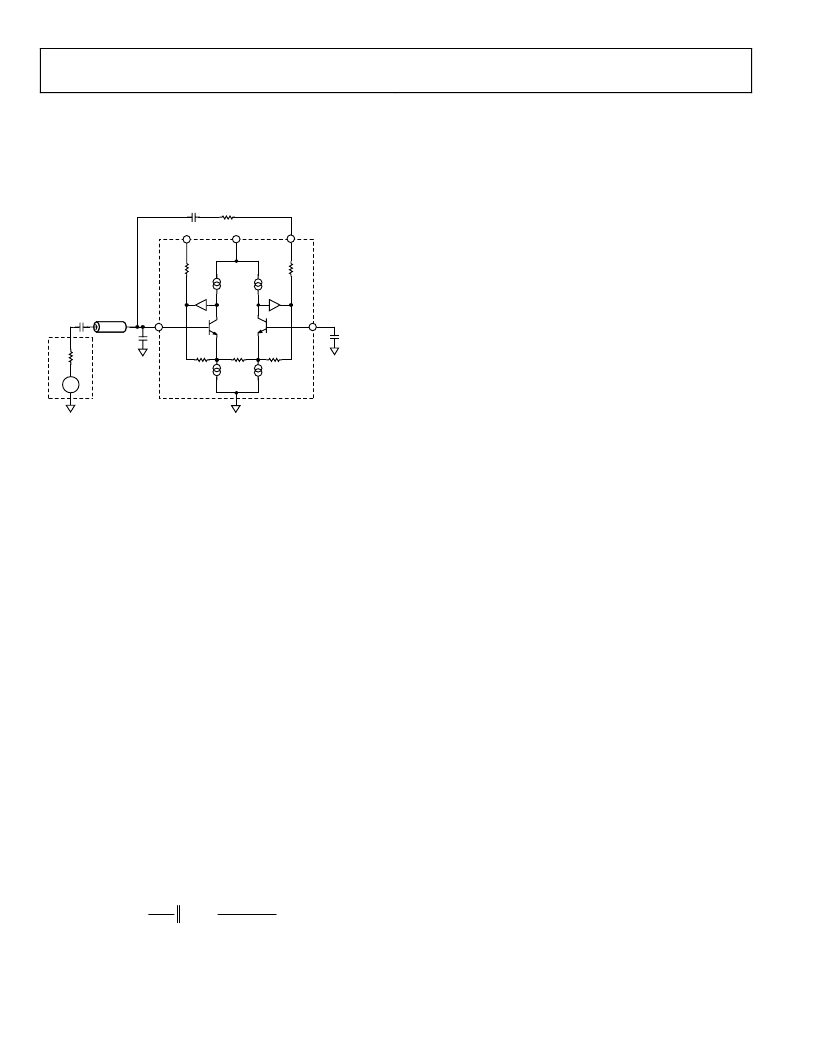
A simplified schematic of the LNA is shown in Figure 59. INH
is capacitively coupled to the source. An on-chip bias generator
centers the output dc levels at 2.5 V and the input voltages at
3.25 V. A capacitor C
LMD
of the same value as the input coupling
capacitor C
INH
is connected from the LMD pin to ground.
Rev. C | Page 18 of 32
VPOS
INH
LOP
LMD
LON
R
S
C
INH
Q1
Q2
I
0
C
LMD
C
SH
R
FB
C
FB
0
I
0
I
0
I
0
Figure 59. Simplified LNA Schematic
The LNA supports differential output voltages as high as
5 V p-p with positive and negative excursions of ±1.25 V, about
a common-mode voltage of 2.5 V. Since the differential gain
magnitude is 9, the maximum input signal before saturation is
± 275 mV or 550 mV p-p. Overload protection ensures quick
recovery time from large input voltages. Since the inputs are
capacitively coupled to a bias voltage near midsupply, very large
inputs can be handled without interacting with the ESD
protection.
Low value feedback resistors and the current-driving capability
of the output stage allow the LNA to achieve a low input-
referred voltage noise of 0.74 nV/√Hz. This is achieved with a
modest current consumption of 10 mA per channel (50 mW).
On-chip resistor matching results in precise gains of 4.5 per side
(9 differential), critical for accurate impedance control. The use
of a fully differential topology and negative feedback minimizes
distortion. Low HD2 is particularly important in second
harmonic ultrasound imaging applications. Differential
signaling enables smaller swings at each output, further
reducing third order distortion.
Active Impedance Matching
The LNA supports active impedance matching through an
external shunt feedback resistor from Pin LON to Pin INH. The
input resistance R
IN
is given by Equation 5, where A is the
single-ended gain of 4.5, and 6 k is the unterminated input
impedance.
( )
5
+
Ω
33
×
Ω
k
6
=
Ω
6
+
1
=
FB
FB
FB
IN
R
R
k
k
A
R
R
C
FB
is needed in series with R
FB
, since the dc levels at Pins LON
and INH are unequal. Expressions for choosing R
FB
in terms of
R
IN
and for choosing C
FB
are found in the Applications section.
C
SH
and the ferrite bead enhance stability at higher frequencies
where the loop gain declines and prevents peaking. Frequency
response plots of the LNA are shown in Figure 19 and Figure 20.
The bandwidth is approximately 130 MHz for matched input
impedances of 50 to 200 and declines at higher source
impedances. The unterminated bandwidth (R
FB
= ∞) is
approximately 80 MHz.
Each output can drive external loads as low as 100 in addition
to the 100 input impedance of the VGA (200 differential).
Capacitive loading up to 10 pF is permissible. All loads should
be ac-coupled. Typically, Pin LOP output is used as a single-
ended driver for auxiliary circuits, such as those used for
Doppler mode ultrasound imaging, and Pin LON drives R
FB
.
Alternatively, a differential external circuit can be driven from
the two outputs, in addition to the active feedback termination.
In both cases, important stability considerations discussed in
the Applications section should be carefully observed.
The impedance at each LNA output is 5 . A 0.4 dB reduction
in open-circuit gain results when driving the VGA, and 0.8 dB
with an additional 100 load at the output. The differential
gain of the LNA is 6 dB higher. If the load is less than 200 on
either side, a compensating load is recommended on the
opposite output.
LNA Noise
The input-referred voltage noise sets an important limit on
system performance. The short-circuit input voltage noise of the
LNA is 0.74 nV/√Hz or 0.82 nV/√Hz (at maximum gain),
including the VGA noise. The open-circuit current noise is
2.5 pA/√Hz. These measurements, taken without a feedback
resistor, provide the basis for calculating the input noise and
noise figure performance of the configurations in Figure 60.
Figure 61 and Figure 62 are simulations extracted from these
results, and the 4.1 dB NF measurement with the input actively
matched to a 50 source. Unterminated (R
FB
= ∞) operation
exhibits the lowest equivalent input noise and noise figure.
Figure 61 shows the noise figure versus source resistance, rising
at low R
S
, where the LNA voltage noise is large compared to the
source noise, and again at high R
S
due to current noise. The
VGA’s input-referred voltage noise of 2.7 nV/√Hz is included in
all of the curves.
相關PDF資料 |
PDF描述 |
|---|---|
| AD8331ARQ-REEL | Ultralow Noise VGAs with Preamplifier and Programmable RIN |
| AD8331ARQ-REEL7 | Ultralow Noise VGAs with Preamplifier and Programmable RIN |
| AD8341 | 1.5 GHz to 2.4 GHz RF Vector Modulator |
| AD8341-EVAL | 1.5 GHz to 2.4 GHz RF Vector Modulator |
| AD8341ACPZ-REEL72 | 1.5 GHz to 2.4 GHz RF Vector Modulator |
相關代理商/技術參數 |
參數描述 |
|---|---|
| AD8332ARU-REEL | 功能描述:IC VGA DUAL W/PREAMP LN 28-TSSOP RoHS:否 類別:集成電路 (IC) >> 線性 - 放大器 - 專用 系列:X-AMP® 產品培訓模塊:Lead (SnPb) Finish for COTS Obsolescence Mitigation Program 標準包裝:60 系列:- 類型:可變增益放大器 應用:CATV 安裝類型:表面貼裝 封裝/外殼:20-WQFN 裸露焊盤 供應商設備封裝:20-TQFN-EP(5x5) 包裝:托盤 |
| AD8332ARU-REEL7 | 功能描述:IC VGA DUAL W/PREAMP LN 28-TSSOP RoHS:否 類別:集成電路 (IC) >> 線性 - 放大器 - 專用 系列:X-AMP® 產品培訓模塊:Lead (SnPb) Finish for COTS Obsolescence Mitigation Program 標準包裝:60 系列:- 類型:可變增益放大器 應用:CATV 安裝類型:表面貼裝 封裝/外殼:20-WQFN 裸露焊盤 供應商設備封裝:20-TQFN-EP(5x5) 包裝:托盤 |
| AD8332ARUZ | 功能描述:IC VGA DUAL W/PREAMP LN 28-TSSOP RoHS:是 類別:集成電路 (IC) >> 線性 - 放大器 - 專用 系列:X-AMP® 產品培訓模塊:Lead (SnPb) Finish for COTS Obsolescence Mitigation Program 標準包裝:60 系列:- 類型:可變增益放大器 應用:CATV 安裝類型:表面貼裝 封裝/外殼:20-WQFN 裸露焊盤 供應商設備封裝:20-TQFN-EP(5x5) 包裝:托盤 |
| AD8332ARUZ | 制造商:Analog Devices 功能描述:IC PRE-AMP ULTRA LOW NOISE |
| AD8332ARUZ-R7 | 功能描述:IC AMP VAR GAIN 2CHAN 28TSSOP RoHS:是 類別:集成電路 (IC) >> 線性 - 放大器 - 專用 系列:X-AMP® 產品培訓模塊:Lead (SnPb) Finish for COTS Obsolescence Mitigation Program 標準包裝:60 系列:- 類型:可變增益放大器 應用:CATV 安裝類型:表面貼裝 封裝/外殼:20-WQFN 裸露焊盤 供應商設備封裝:20-TQFN-EP(5x5) 包裝:托盤 |
發布緊急采購,3分鐘左右您將得到回復。