- 您現在的位置:買賣IC網 > PDF目錄360984 > IS42S16800A-10BI 16Meg x 8, 8Meg x16 & 4Meg x 32 128-MBIT SYNCHRONOUS DRAM PDF資料下載
參數資料
| 型號: | IS42S16800A-10BI |
| 英文描述: | 16Meg x 8, 8Meg x16 & 4Meg x 32 128-MBIT SYNCHRONOUS DRAM |
| 中文描述: | 16Meg × 8,8Meg x16 |
| 文件頁數: | 31/66頁 |
| 文件大小: | 556K |
| 代理商: | IS42S16800A-10BI |
第1頁第2頁第3頁第4頁第5頁第6頁第7頁第8頁第9頁第10頁第11頁第12頁第13頁第14頁第15頁第16頁第17頁第18頁第19頁第20頁第21頁第22頁第23頁第24頁第25頁第26頁第27頁第28頁第29頁第30頁當前第31頁第32頁第33頁第34頁第35頁第36頁第37頁第38頁第39頁第40頁第41頁第42頁第43頁第44頁第45頁第46頁第47頁第48頁第49頁第50頁第51頁第52頁第53頁第54頁第55頁第56頁第57頁第58頁第59頁第60頁第61頁第62頁第63頁第64頁第65頁第66頁
Integrated Silicon Solution, Inc. — www.issi.com —
1-800-379-4774
ADVANCED INFORMATION
Rev. 00A
06/01/02
31
ISSI
IS42S81600A, IS42S16800A, IS42S32400A
IS42LS81600A, IS42LS16800A, IS42LS32400A
DON'T CARE
UNDEFINED
CLK
COMMAND
DQ
READ
NOP
NOP
NOP
CAS Latency - 3
t
AC
t
OH
D
OUT
T0
T1
T2
T3
T4
t
LZ
CLK
COMMAND
DQ
READ
NOP
NOP
CAS Latency - 2
t
AC
t
OH
D
OUT
T0
T1
T2
T3
t
LZ
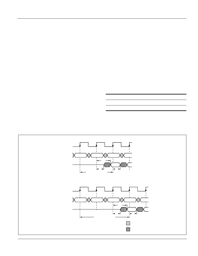
CAS LATENCY
CAS Latency
The CAS latency is the delay, in clock cycles, between the
registration of a READ command and the availability of the
first piece of output data. The latency can be set to two or
three clocks.
If a READ command is registered at clock edge n, and the
latency is
m
clocks, the data will be available by clock edge
n +
m. The DQs will start driving as a result of the clock edge
one cycle earlier
(n + m
- 1), and provided that the relevant
access times are met, the data will be valid by clock edge
n +
m. For example, assuming that the clock cycle time is
such that all relevant access times are met, if a READ
command is registered at T0 and the latency is programmed
to two clocks, the DQs will start driving after T1 and the data
will be valid by T2, as shown in CAS Latency diagrams. The
Allowable Operating Frequency table indicates the operat-
ing frequencies at which each CAS latency setting can be
used.
Reserved states should not be used as unknown operation or
incompatibility with future versions may result.
Operating Mode
The normal operating mode is selected by setting M7 and M8
to zero; the other combinations of values for M7 and M8 are
CAS Latency
Allowable Operating Frequency (MHz)
Speed
CAS Latency = 2
CAS Latency = 3
7.5
100
133
10
75
100
reserved for future use and/or test modes. The programmed
burst length applies to both READ and WRITE bursts.
Test modes and reserved states should not be used
because unknown operation or incompatibility with future
versions may result.
Write Burst Mode
When M9 = 0, the burst length programmed via M0-M2
applies to both READ and WRITE bursts; when M9 = 1, the
programmed burst length applies to READ bursts, but write
accesses are single-location (nonburst) accesses.
相關PDF資料 |
PDF描述 |
|---|---|
| IS42S32400A-10BI | 16Meg x 8, 8Meg x16 & 4Meg x 32 128-MBIT SYNCHRONOUS DRAM |
| IS42LS81600A-10T | 16Meg x 8, 8Meg x16 & 4Meg x 32 128-MBIT SYNCHRONOUS DRAM |
| IS42LS32400A-10T | 16Meg x 8, 8Meg x16 & 4Meg x 32 128-MBIT SYNCHRONOUS DRAM |
| IS42S32400A-10T | 16Meg x 8, 8Meg x16 & 4Meg x 32 128-MBIT SYNCHRONOUS DRAM |
| IS42S32400A-10TI | 16Meg x 8, 8Meg x16 & 4Meg x 32 128-MBIT SYNCHRONOUS DRAM |
相關代理商/技術參數 |
參數描述 |
|---|---|
| IS42S16800A-10T | 制造商:Integrated Silicon Solution Inc 功能描述:DRAM Chip SDRAM 128M-Bit 8Mx16 3.3V 54-Pin TSOP-II |
| IS42S16800A-10TI | 制造商:ICSI 制造商全稱:Integrated Circuit Solution Inc 功能描述:16Meg x 8, 8Meg x16 & 4Meg x 32 128-MBIT SYNCHRONOUS DRAM |
| IS42S16800A-10TL | 制造商:ISSI 制造商全稱:Integrated Silicon Solution, Inc 功能描述:16Meg x 8, 8Meg x16 & 4Meg x 32 128-MBIT SYNCHRONOUS DRAM |
| IS42S16800A-10TLI | 制造商:ISSI 制造商全稱:Integrated Silicon Solution, Inc 功能描述:16Meg x 8, 8Meg x16 & 4Meg x 32 128-MBIT SYNCHRONOUS DRAM |
| IS42S16800A1-7TL | 制造商:ISSI 制造商全稱:Integrated Silicon Solution, Inc 功能描述:8Meg x16 128-MBIT SYNCHRONOUS DRAM |
發布緊急采購,3分鐘左右您將得到回復。