- 您現在的位置:買賣IC網 > PDF目錄361024 > LM2421 (National Semiconductor Corporation) Monolithic Triple Channel HDTV Driver PDF資料下載
參數資料
| 型號: | LM2421 |
| 廠商: | National Semiconductor Corporation |
| 英文描述: | Monolithic Triple Channel HDTV Driver |
| 中文描述: | 單片驅動三高清晰度電視頻道 |
| 文件頁數: | 2/13頁 |
| 文件大小: | 998K |
| 代理商: | LM2421 |
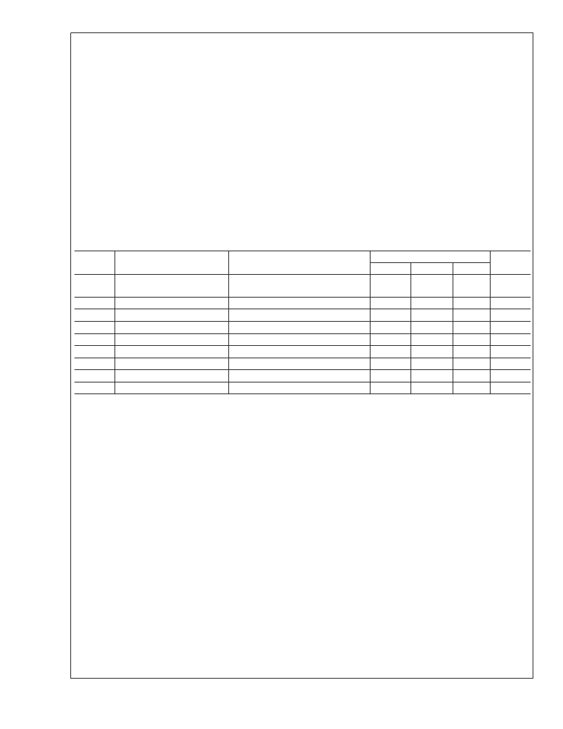
Absolute Maximum Ratings
(Notes 1, 3)
If Military/Aerospace specified devices are required,
please contact the National Semiconductor Sales Office/
Distributors for availability and specifications.
Supply Voltage (V
CC
)
Bias Voltage (V
BB
)
Input Voltage (V
IN
)
Storage Temperature Range (T
STG
)
+155V
+15V
-0.5V to V
BB
+0.5V
65C to +150C
Lead Temperature
(Soldering,
<
10 sec.)
ESD Tolerance, Human Body Model
Machine Model
Junction Temperature
θ
JC
(typ)
300C
2kV
200V
150C
2.8C/W
Operating Ranges
(Note 2)
V
CC
V
BB
V
IN
V
OUT
Do not operate the part without a heat sink.
+130V to +150V
+7V to +13V
+1V to +5V
+16V to +135V
Electrical Characteristics
(See Figure 2 for Test Circuit)
Unless otherwise noted: V
CC
= +145V, V
BB
= +8V, C
L
= 8 pF, T
C
= 50C
DC Tests: V
= 2.8VDC
AC Tests: Output = 100V
PP
(32V - 132V) at 1MHz
Symbol
Parameter
Conditions
LM2421
Typical
Units
Min
Max
I
CC
Supply Current
All Three Channels, No Input Signal,
No Output Load
All Three Channels
No AC Input Signal
No AC Input Signal
(Note 4), No AC Input Signal
(Notes 4, 5), No AC Input Signal
(Note 6), 10% to 90%
(Note 6), 90% to 10%
(Note 6)
43
55
mA
I
BB
V
OUT
A
V
A
V
LE
t
R
t
F
OS
Bias Current
DC Output Voltage
DC Voltage Gain
Gain Matching
Linearity Error
Rise Time
Fall Time
Overshoot
29
82
42
1.0
8
11
13
2
40
86
46
mA
V
DC
78
38
dB
%
ns
ns
%
Note 1:
Absolute Maximum Ratings indicate limits beyond which damage to the device may occur.
Note 2:
Operating ratings indicate conditions for which the device is functional, but do not guarantee specific performance limits. For guaranteed specifications and
test conditions, see the Electrical Characteristics. Datasheet min/max specification limits are guaranteed by design, test, or statistical analysis. The guaranteed
specifications apply only for the test conditions listed. Some performance characteristics may change when the device is not operated under the listed test
conditions.
Note 3:
All voltages are measured with respect to GND, unless otherwise specified.
Note 4:
Calculated value from Voltage Gain test on each channel.
Note 5:
Linearity Error is the variation in dc gain from V
IN
= 1.8V to V
IN
= 3.8V.
Note 6:
Input from signal generator: t
r
, t
f
<
1 ns.
L
www.national.com
2
相關PDF資料 |
PDF描述 |
|---|---|
| LM2476 | Monolithic Triple Channel 6.5 ns High Gain CRT Driver and Bias Clamp |
| LM2480 | RES 91 OHM 1/2W 5% CARBON FILM |
| LM2480NA | RES 9.1K OHM 1/2W 5% CARBON FILM |
| LM24 | Monolithic Triple 9.5 ns CRT Driver |
| LM2409 | Monolithic Triple 9.5 ns CRT Driver |
相關代理商/技術參數 |
參數描述 |
|---|---|
| LM242-155.52M | 制造商:CONNOR-WINFIELD 制造商全稱:Connor-Winfield Corporation 功能描述:5.0x7.0mm Surface Mount LVDS Clock Oscillator Series |
| LM2421AT WAF | 制造商:Texas Instruments 功能描述: |
| LM2421TA | 制造商:NSC 制造商全稱:National Semiconductor 功能描述:Monolithic Triple Channel HDTV Driver |
| LM2422 | 制造商:NSC 制造商全稱:National Semiconductor 功能描述:220V Monolithic Triple Channel 30 MHz CRT DTV Driver |
| LM2422_0505 | 制造商:NSC 制造商全稱:National Semiconductor 功能描述:220V Monolithic Triple Channel 30 MHz CRT DTV Driver |
發布緊急采購,3分鐘左右您將得到回復。