- 您現(xiàn)在的位置:買賣IC網(wǎng) > PDF目錄361025 > LM2743 (National Semiconductor Corporation) N-Channel FET Synchronous Buck Regulator Controller for Conversion from 3.3V PDF資料下載
參數(shù)資料
| 型號: | LM2743 |
| 廠商: | National Semiconductor Corporation |
| 英文描述: | N-Channel FET Synchronous Buck Regulator Controller for Conversion from 3.3V |
| 中文描述: | N溝道場效應(yīng)管同步降壓穩(wěn)壓控制器,用于從3.3V轉(zhuǎn)換 |
| 文件頁數(shù): | 15/23頁 |
| 文件大小: | 653K |
| 代理商: | LM2743 |
Application Information
(Continued)
In this example, in order to maintain a 2% peak-to-peak
output voltage ripple and a 40% peak-to-peak inductor cur-
rent ripple, the required maximum ESR is 15m
.The Sanyo
4SP560M aluminum electrolytic capacitor will give an
equivalent ESR of 14m
. The capacitance of 560μF is
enough to supply even severe load transients.
MOSFETs
MOSFETs are the critical parts of any switching controller.
Both, the control high side FET and the synchronous low
side FET, have a direct impact on the system efficiency.
In this case the target efficiency for typical application circuit
is about 89%. This variable will determine which MOSFET is
acceptable to use for the design.
Loss from the capacitors, inductors, and IC come to about
0.27W. This leaves about 0.33W for the FET switching,
conduction, and gate charging losses to meet the target
efficiency.All the losses are detailed in the Efficiency section.
The switching loss is particularly difficult to estimate because
it depends on many factors. When the load current is more
than about 1 or 2 amps, conduction losses outweigh the
switching and gate charging losses. This allows FET selec-
tion based on the R
DS(ON)
of the FET. After adding the FET
switching and gate charging losses about 0.27W leaves for
conduction losses. When plugged MOSFET, the FDS6898A
with a typical R
DS(ON)
of 13m
, into the equation from Effi-
ciency section for P
CND
the loss come to be about 0.27W.
Control Loop Components
The Typical Application Circuit has been compensated to
improve the DC gain and bandwidth. The result of this com-
pensation is better line and load transient responses. For the
LM2743, the top feedback divider resistor, R
, is also a
part of the compensation. For the 3.3V to 1.2V at 4A design,
the values are:
C
C1
= 27pF, C
= 1200nF, C
C3
= 3300pF, R
C1
= 40.2k
,
R
C2
= 2.55k
, R
FB2
= 10k
.
These values give a phase margin of 53 and a bandwidth of
80kHz.
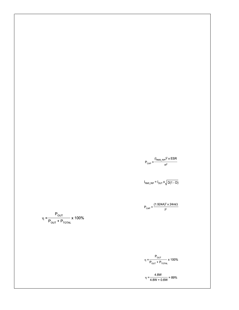
EFFICIENCY CALCULATIONS
A reasonable estimation of the efficiency of a switching buck
controller can be obtained by adding together the Output
Power (P
OUT
) loss and the Total Power (P
TOTAL
) loss:
The Output Power (P
) for theTypical Application Circuit
design is (1.2V * 4A) = 4.8W. The Total Power (P
), with
an efficiency calculation to complement the design, is shown
below.
The majority of the power losses are due to low and high
side of MOSFET’s losses. The losses in any MOSFET are
group of switching (P
SW
) and conduction losses(P
CND
).
P
FET
= P
SW
+ P
CND
= 61.38mW + 270mW
P
FET
= 331.4mW
FET Switching Loss (P
SW
)
P
SW
= P
SW(ON)
+ P
SW(OFF)
P
SW
= 0.5 * V
CC
* I
OUT
* (t
r
+ t
f
)* F
OSC
P
SW
= 0.5 x 3.3V x 4A x 300kHz x 31ns
P
SW
= 61.38mW
The FDS6898A has a typical turn-on rise time t
and turn-off
fall time t
of 15ns and 16ns, respectively. The switching
losses for this type of dual N-Channel MOSFETs are
0.061W.
FET Conduction Loss (P
CND
)
P
CND
= P
CND1
+ P
CND2
P
CND1
= I
2OUT
x R
DS(ON)
x k x D
P
CND2
= I
2OUT
x R
DS(ON)
x k x (1-D)
R
DS(ON)
= 13m
and the factor is a constant value (k = 1.3)
to account for the increasing R
DS(ON)
of a FET due to heat-
ing.
P
CND1
= (4A)
2
x 13m
x 1.3 x 0.364
P
CND2
= (4A)
2
x 13m
x 1.3 x (1 - 0.364)
P
CND
= 98.42mW + 172mW = 270mW
There are few additional losses that are taken into account:
IC Operating Loss (P
IC)
P
IC
= I
Q_VCC
x V
CC
,
where I
Q-VCC
is the typical operating V
CC
current
P
IC
= 1.5mA *3.3V = 4.95mW
FET Gate Charging Loss (P
GATE
)
P
GATE
= n * V
CC
* Q
GS
* F
OSC
P
GATE
= 2 x 3.3V x 3nC x 300kHz
P
GATE
= 5.94mW
The value n is the total number of FETs used and Q
is the
typical gate-source charge value, which is 3nC. For the
FDS6898A the gate charging loss is 5.94mW.
Input Capacitor Loss (P
CAP
)
Where,
n is the number of capacitors, and ESR is equivalent series
resistance.
P
CAP
= 88.8mW
Output Inductor Loss (P
IND
)
P
IND
= I
2OUT
* DCR
IOUT
,
where DCR
IOUT
is the direct current resistance
P
IND
= (4A)
2
x 11m
P
IND
= 176mW
Total System Efficiency
L
www.national.com
15
相關(guān)PDF資料 |
PDF描述 |
|---|---|
| LM2744 | Low Voltage N-Channel MOSFET Synchronous Buck Regulator Controller with External Reference |
| LM2796TL | Dual-Display White LED Driver with 3/2x Switched Capacitor Boost |
| LM2796TLX | Dual-Display White LED Driver with 3/2x Switched Capacitor Boost |
| LM2796 | Dual-Display White LED Driver with 3/2x Switched Capacitor Boost |
| LM2925 | Cap-Free, NMOS, 150mA Low Dropout Regulator with Reverse Current Protection |
相關(guān)代理商/技術(shù)參數(shù) |
參數(shù)描述 |
|---|---|
| LM2743-19AEVAL | 功能描述:電源管理IC開發(fā)工具 LM2743 EVAL BOARD RoHS:否 制造商:Maxim Integrated 產(chǎn)品:Evaluation Kits 類型:Battery Management 工具用于評估:MAX17710GB 輸入電壓: 輸出電壓:1.8 V |
| LM2743EVAL | 功能描述:BOARD EVALUATION LM2743 RoHS:否 類別:編程器,開發(fā)系統(tǒng) >> 評估板 - DC/DC 與 AC/DC(離線)SMPS 系列:PowerWise® 產(chǎn)品培訓(xùn)模塊:Obsolescence Mitigation Program 標(biāo)準(zhǔn)包裝:1 系列:True Shutdown™ 主要目的:DC/DC,步升 輸出及類型:1,非隔離 功率 - 輸出:- 輸出電壓:- 電流 - 輸出:1A 輸入電壓:2.5 V ~ 5.5 V 穩(wěn)壓器拓?fù)浣Y(jié)構(gòu):升壓 頻率 - 開關(guān):3MHz 板類型:完全填充 已供物品:板 已用 IC / 零件:MAX8969 |
| LM2743EVAL/NOPB | 功能描述:電源管理IC開發(fā)工具 LM2743 EVAL BOARD RoHS:否 制造商:Maxim Integrated 產(chǎn)品:Evaluation Kits 類型:Battery Management 工具用于評估:MAX17710GB 輸入電壓: 輸出電壓:1.8 V |
| LM2743MTC | 功能描述:DC/DC 開關(guān)控制器 RoHS:否 制造商:Texas Instruments 輸入電壓:6 V to 100 V 開關(guān)頻率: 輸出電壓:1.215 V to 80 V 輸出電流:3.5 A 輸出端數(shù)量:1 最大工作溫度:+ 125 C 安裝風(fēng)格: 封裝 / 箱體:CPAK |
| LM2743MTC/NOPB | 功能描述:DC/DC 開關(guān)控制器 RoHS:否 制造商:Texas Instruments 輸入電壓:6 V to 100 V 開關(guān)頻率: 輸出電壓:1.215 V to 80 V 輸出電流:3.5 A 輸出端數(shù)量:1 最大工作溫度:+ 125 C 安裝風(fēng)格: 封裝 / 箱體:CPAK |
發(fā)布緊急采購,3分鐘左右您將得到回復(fù)。