- 您現在的位置:買賣IC網 > PDF目錄361036 > LM98501 (National Semiconductor Corporation) 10-Bit, 27 MSPS Camera Signal Processor PDF資料下載
參數資料
| 型號: | LM98501 |
| 廠商: | National Semiconductor Corporation |
| 英文描述: | 10-Bit, 27 MSPS Camera Signal Processor |
| 中文描述: | 10位,27 MSPS的攝像機信號處理器 |
| 文件頁數: | 16/24頁 |
| 文件大小: | 490K |
| 代理商: | LM98501 |
System Overview
(Continued)
COLOR FILTER ARRAY (CFA) CONFIGURATION
In order to utilize the LM98501’s programmable pixel-rate
gain, a color filter array (CFA) pattern must be defined. Some
commonly used CFA patterns are as follows:
Bayer Pattern
Red
Green
Line 0
Line 1
Green
Blue
Green
Blue
Red
Green
CMYG Pattern
Magenta
Green
Line 0
Line 1
Therefore, two 8-bit words must be written to the CFA line
registers to specify the CFA pattern being used. Also, two
2-bit numbers must be written to the CFA definition register
indicating the number of pixels per pattern in each line of the
defined CFA pattern. The information contained in the CFA
line registers indicates the registers where the respective
PGA gain and offset values are stored. For example, a sys-
tem using the Bayer pattern defined above would first write
four PGAgains and their respective offsets into the four PGA
gain and four analog offset registers. Next, two 8-bit words
(one word/CFA line) would be written to the CFA configura-
tion registers. The 8-bit CFA configuration words each con-
sist of four 2-bit numbers, each of which is the address for
the gain and offset values of the color that appears in that lo-
cation in the CFA line. Finally, two 2-bit numbers specifying
the number of elements in each CFAline must be written into
the CFAdefinition register.ACFAconfiguration will then con-
tain four 2-bit numbers indicating the registers where the
gain and offset values are located for a maximum of four col-
ors on each CFA line. In addition, the CFA definition register
will contain two 2-bit numbers that designate the number of
elements used in each CFA line for the particular CFA pat-
tern being applied to the system.
Example A contains a CFA pattern that repeats the colors
cyan and magenta on the first line, and repeats the pattern
blue, green, green, blue on the second line. Each 2-bit num-
ber in the CFA line registers refers to a common set of PGA
gain and offset registers for each color. The first line indi-
Cyan
Cyan
Yellow
Yellow
Green
Magenta
cates that the color magenta uses the gain and offset values
stored in PGA gain register 1 (address 1h) and analog offset
register 1 (address 5h). Also, the first line indicates that the
color cyan uses the gain and offset values in PGA gain reg-
ister 2 (address 2h) and analog offset register 2 (address
6h). The second line indicates gain and offset values for the
color blue and the color green in the same fashion as the first
line.
Example A
7
XX
11
00
0
CFA Line 0
CFA Line 1
CFA Definition
In addition to specifying the gain and offset for each line, it is
also necessary to specify the number of elements contained
in each CFAline’s pixel pattern. The CFAdefinition register is
used to store this value (number of elements per line). In ex-
ample A, the user has stored the 2-bit binary number
01
into
the CFA definition register’s two LSB’s indicating that the
pattern in line 0 contains two repeating colors or elements.
Also, the 2-bit binary number
11
has been written into bit 2
and bit 3 of the CFA definition register indicating that the re-
spective CFA pattern contains four repeating colors or ele-
ments, as the colors blue and green alternate position in the
example pattern.
Once both lines for the pattern have been stored, it is applied
when the beginning of line (BOL) signal is asserted by the
user. One line of the CFA pattern is applied repeatedly until
the BOL signal is reset (at the end of the current line). Once
the BOL signal is set again, the CFA line information is
changed from that defined by the CFA line 0 register to that
defined by the CFA line 1 register and the process starts
again. For more details of the timing of the BOL signal,
please refer to Figure 6
XX
00
00
01
00
11
10
11
01
SOFTWARE CONTROL
There are two software control registers accessible via the
serial interface. The software control registers are divided
into customer (register 0) and advanced (register 1) func-
tions. Please refer to the register data descriptions for more
information on the software control registers.
POWER LEVEL CONTROL
The LM98501 is equipped with two power trim registers that
may be used to adjust power levels of various circuits inter-
nal to the device. In its default condition, the LM98501 is set
for optimum power and performance, and modifying the val-
ues stored in the power level control registers will affect per-
formance as a result of the change in power level(s). In ap-
plications where maximum performance is desired, the
default values should be used. Otherwise, power levels may
be decreased at the slight expense of performance. Please
refer to the register data descriptions for more information
regarding the power level control registers.
The ADC coarse and fine bank power adjustment bits are lo-
cated in the power level control 2 register, bits 7:4. Altering
these bits may significantly affect performance and power
dissipation. Please see “DNL vs. Power Control Setting
@
27 MHz Clock Frequency” and “Power Dissipation vs. Power
Control Setting” on page 11.
DS101292-37
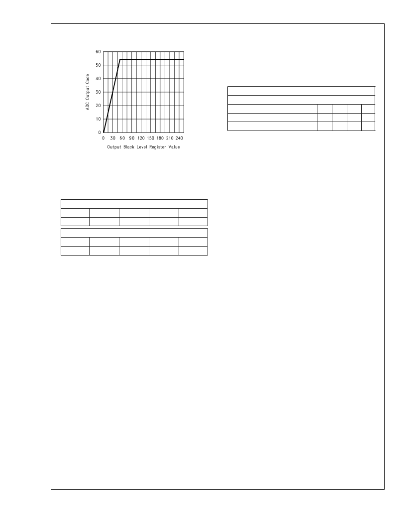
FIGURE 11. ADC Output vs. Black Level Register Value
L
www.national.com
16
相關PDF資料 |
PDF描述 |
|---|---|
| LMC555CBPEVAL | CMOS Timer |
| LMC555CN | CMOS Timer |
| LMC555 | CMOS Timer |
| LMC555CM | CMOS Timer |
| LMC555CMM | CMOS Timer |
相關代理商/技術參數 |
參數描述 |
|---|---|
| LM98501A WAF | 制造商:Texas Instruments 功能描述: |
| LM98501CCVBH | 制造商:NSC 制造商全稱:National Semiconductor 功能描述:10-Bit, 27 MSPS Camera Signal Processor |
| LM98501VBH WAF | 制造商:Texas Instruments 功能描述: |
| LM98502A WAF | 制造商:Texas Instruments 功能描述: |
| LM98503 | 制造商:NSC 制造商全稱:National Semiconductor 功能描述:10-Bit, 18 MSPS Camera Signal Processor |
發布緊急采購,3分鐘左右您將得到回復。