- 您現在的位置:買賣IC網 > Datasheet目錄41 > LT3507HUHF#TRPBF (Linear Technology)IC REG QD BUCK/LINEAR 38-QFN Datasheet資料下載
參數資料
| 型號: | LT3507HUHF#TRPBF |
| 廠商: | Linear Technology |
| 文件頁數: | 16/28頁 |
| 文件大小: | 302K |
| 描述: | IC REG QD BUCK/LINEAR 38-QFN |
| 產品培訓模塊: | More Information on LDOs |
| 標準包裝: | 2,500 |
| 拓撲: | 降壓(降壓)(1),線性(LDO)(1) |
| 功能: | 任何功能 |
| 輸出數: | 4 |
| 頻率 - 開關: | 900kHz ~ 1.1MHz |
| 電壓/電流 - 輸出 1: | 0.8 V ~ 32.4 V,2.4A |
| 電壓/電流 - 輸出 2: | 0.8 V ~ 32.4 V,1.5A |
| 電壓/電流 - 輸出 3: | 0.8 V ~ 32.4 V,1.5A |
| 帶 LED 驅動器: | 無 |
| 帶監控器: | 無 |
| 帶序列發生器: | 是 |
| 電源電壓: | 4 V ~ 36 V |
| 工作溫度: | -40°C ~ 150°C |
| 安裝類型: | 表面貼裝 |
| 封裝/外殼: | 38-WFQFN 裸露焊盤 |
| 供應商設備封裝: | 38-QFN(5x7) |
| 包裝: | 帶卷 (TR) |
第1頁第2頁第3頁第4頁第5頁第6頁第7頁第8頁第9頁第10頁第11頁第12頁第13頁第14頁第15頁當前第16頁第17頁第18頁第19頁第20頁第21頁第22頁第23頁第24頁第25頁第26頁第27頁第28頁
LT3507
16
3507fa
Frequency Compensation
The LT3507 uses current mode control to regulate the
output. This simpli es loop compensation. In particular, the
LT3507 does not depend on the ESR of the output capacitor
for stability so you are free to use ceramic capacitors to
achieve low output ripple and small circuit size.
The components tied to the V
C
pin provide frequency
compensation. Generally, a capacitor and a resistor in
series to ground determine loop gain. In addition, there
is a lower value capacitor in parallel. This capacitor lters
noise at the switching frequency and is not part of the
loop compensation.
Loop compensation determines the stability and transient
performance. Designing the compensation network is a bit
complicated and the best values depend on the application
and the type of output capacitor. A practical approach is to
start with one of the circuits in this data sheet that is similar
to your application and tune the compensation network
to optimize the performance. Check stability across all
operating conditions, including load current, input voltage
and temperature. The LT1375 data sheet contains a more
thorough discussion of loop compensation and describes
how to test the stability using a transient load. Application
Note 76 is an excellent source as well.
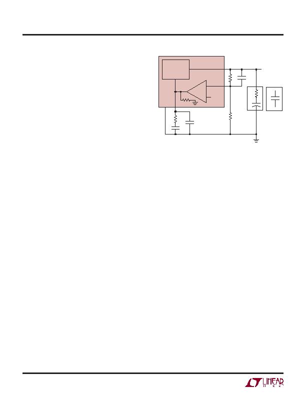
Figure 6 shows an equivalent circuit for the LT3507 control
loop. The error amp is a transconductance ampli er with
nite output impedance. The power section, consisting of
the modulator, power switch and inductor is modeled as a
transconductance ampli er generating an output current
proportional to the voltage at the V
C
pin. The gain of the
power stage (g
mp
) is 5S for Channel 1 and 3.6S for Chan-
nels 2 and 3. Note that the output capacitor integrates this
current and that the capacitor on the V
C
pin (C
C
) integrates
the error ampli er output current, resulting in two poles
in the loop. In most cases, a zero is required and comes
either from the output capacitor ESR or from a resistor
in series with C
C
. This model works well as long as the
inductor current ripple is not too low (擨
RIPPLE
> 5% I
OUT
)
and the loop crossover frequency is less than f
SW
/5. A
phase lead capacitor (C
PL
) across the feedback divider
may improve the transient response.
SHUTDOWN
The RUN pins are used to place the individual switch-
ing regulators and the internal bias circuits in shutdown
mode. When all three RUN pins are pulled low, the LT3507
is in shutdown mode and draws less than 1糀 from the
input supply. When any RUN pin is pulled high (>1.5V)
the internal reference, LDO and selected channel are all
turned on.
The RUN pins draw a small amount of current to power
the reference. The current is less than 3糀 at 1.8V, so the
RUN pin can be driven directly from 1.8V logic. The RUN
pins are rated up to 36V and can be connected directly to
the input voltage.
A RUN pin cannot be pulled up by logic powered by its
own output, i.e., RUN1 cant be pulled up by logic powered
by OUT1.
POWER GOOD INDICATORS
The PGOOD pin is the open-collector output of an internal
comparator. PGOOD remains low until the FB pin is within
10% of the nal regulation voltage. Tie the PGOOD to any
supply with a pull-up resistor that will supply less than
200糀. Note that this pin will be open when the LT3507 is
in shutdown mode (all three RUN pins at ground) regard-
less of the voltage at the FB pin. PGOOD is valid when
the LT3507 is enabled (any RUN pin is high) and V
IN
is
greater than ~3.5V.
APPLICATIONS INFORMATION
Figure 6. Loop Response Model
V
FB
800mV
V
SW
V
C
LT3507
GND
3507 F06
R1
OUTPUT
ESR
C
F
C
C
R
C
500k
ERROR
AMPLIFIER
FB
R2
C1
C1
CURRENT MODE
POWER STAGE
g
mp
330糞
+
POLYMER
OR
TANTALUM
CERAMIC
C
PL
相關PDF資料 |
PDF描述 |
|---|---|
| LT3570IFE#TRPBF | IC REG BUCK/BST/LINEAR 20TSSOP |
| LT3645HMSE#TRPBF | IC REG DL BUCK/LINEAR 12-MSOP |
| LT3694IFE-1#TRPBF | IC REG TRPL BUCK/LINEAR 20TSSOP |
| LT4220IGN#TR | IC CTLR HOTSWAP DUAL 16-SSOP |
| LT4250LCN8 | IC CONTRLR HOT SWAP NEG 48V 8DIP |
相關代理商/技術參數 |
參數描述 |
|---|---|
| LT3507IUHF#PBF | 功能描述:IC REG QD BUCK/LINEAR 38-QFN RoHS:是 類別:集成電路 (IC) >> PMIC - 穩壓器 - 線性 + 切換式 系列:- 標準包裝:2,500 系列:- 拓撲:降壓(降壓)同步(3),線性(LDO)(2) 功能:任何功能 輸出數:5 頻率 - 開關:300kHz 電壓/電流 - 輸出 1:控制器 電壓/電流 - 輸出 2:控制器 電壓/電流 - 輸出 3:控制器 帶 LED 驅動器:無 帶監控器:無 帶序列發生器:是 電源電壓:5.6 V ~ 24 V 工作溫度:-40°C ~ 85°C 安裝類型:* 封裝/外殼:* 供應商設備封裝:* 包裝:* |
| LT3507IUHF#TRPBF | 功能描述:IC REG QD BUCK/LINEAR 38-QFN RoHS:是 類別:集成電路 (IC) >> PMIC - 穩壓器 - 線性 + 切換式 系列:- 標準包裝:2,500 系列:- 拓撲:降壓(降壓)同步(3),線性(LDO)(2) 功能:任何功能 輸出數:5 頻率 - 開關:300kHz 電壓/電流 - 輸出 1:控制器 電壓/電流 - 輸出 2:控制器 電壓/電流 - 輸出 3:控制器 帶 LED 驅動器:無 帶監控器:無 帶序列發生器:是 電源電壓:5.6 V ~ 24 V 工作溫度:-40°C ~ 85°C 安裝類型:* 封裝/外殼:* 供應商設備封裝:* 包裝:* |
| LT3507IUHFPBF | 制造商:Linear Technology 功能描述:Triple Voltage Regulator QFN38EP |
| LT3507IUHF-PBF | 制造商:LINER 制造商全稱:Linear Technology 功能描述:Triple Monolithic Step-Down Regulator with LDO |
| LT3507IUHF-TRPBF | 制造商:LINER 制造商全稱:Linear Technology 功能描述:Triple Monolithic Step-Down Regulator with LDO |
發布緊急采購,3分鐘左右您將得到回復。