- 您現在的位置:買賣IC網 > Datasheet目錄42 > MAX1765EUE+ (Maxim Integrated)IC REG DL BST/LINEAR 16TSSOP Datasheet資料下載
參數資料
| 型號: | MAX1765EUE+ |
| 廠商: | Maxim Integrated |
| 文件頁數: | 10/19頁 |
| 文件大小: | 867K |
| 描述: | IC REG DL BST/LINEAR 16TSSOP |
| 產品培訓模塊: | Lead (SnPb) Finish for COTS Obsolescence Mitigation Program |
| 標準包裝: | 96 |
| 拓撲: | 升壓(升壓)同步(1),線性(LDO)(1) |
| 功能: | 任何功能 |
| 輸出數: | 2 |
| 頻率 - 開關: | 1MHz |
| 電壓/電流 - 輸出 1: | 2.5 V ~ 5.5 V,800mA |
| 電壓/電流 - 輸出 2: | 2.85V/可調,500mA |
| 帶 LED 驅動器: | 無 |
| 帶監控器: | 無 |
| 帶序列發生器: | 無 |
| 電源電壓: | 0.7 V ~ 5.5 V |
| 工作溫度: | -40°C ~ 85°C |
| 安裝類型: | 表面貼裝 |
| 封裝/外殼: | 16-TSSOP(0.173",4.40mm)裸露焊盤 |
| 供應商設備封裝: | 16-TSSOP-EP |
| 包裝: | 管件 |
Detailed Description
The MAX1765 is a highly efficient, low-noise power
supply for portable RF hand-held instruments. This
boost power supply combines an LDO linear regulator,
a low-noise, high-power, step-up switching regulator,
an N-channel power MOSFET, a P-channel synchro-
nous rectifier, shutdown control, and a precision volt-
age reference in a single 16-pin QSOP or a thermally
enhanced TSSOP-EP (Figure 1).
The switching DC-DC converter boosts a 1-cell to 3-cell
NiMH/NiCd or a single Li+ battery input to an adjustable
output voltage between 2.5V and 5.5V. The MAX1765
guarantees startup with voltages as low as 1.1V and will
remain operational down to 0.7V (Figure 2). The internal
LDO regulator provides linear postregulation for noise-
sensitive circuitry, or it can be used as a separate volt-
age output adjustable from 1.25V up to POUT.
The MAX1765 is optimized for use in cellular phones and
other applications requiring low noise during full-power
operation, as well as low quiescent current for maximum
battery life during standby and shutdown. The device
automatically transitions to a low-quiescent-current
pulse-skipping control scheme during light loads that
reduces the quiescent power consumption to 360礧.
The supply current of the device can be further reduced
to 1礎 when the device is shut down. Figure 2 shows a
typical application of the MAX1765 in normal mode.
The switching regulator supports two low-noise modes:
fixed-frequency PWM for low noise in all load conditions,
and synchronization of the internal oscillator to an
external clock driving the CLK input. In TRACK mode,
the DC and linear regulator work together to maintain
excellent PSRR without excessive efficiency loss.
Additional MAX1765 features include synchronous rec-
tification for high efficiency and increased battery life,
dual boost shutdown controls for 礟 or a pushbutton
momentary switch, and a separate shutdown control for
the linear regulator.
Step-Up Converter
During DC-DC converter operation, the internal N-chan-
nel MOSFET turns on for the first part of each cycle,
allowing current to ramp up in the inductor and store
energy in a magnetic field. During the second part of
each cycle, the MOSFET turns off and inductor current
flows through the synchronous rectifier to the output filter
capacitor and the load. As the energy stored in the
inductor is depleted, the current ramps down and the
synchronous rectifier turns off. The CLK/SEL pin deter-
mines whether a pulse-skipping or PWM control method
is used at light loads (Table 1).
Normal Operation
Pulling CLK/SEL low selects the MAX1765s normal
operating mode. In this mode, the device operates in
PWM when driving medium to heavy loads and auto-
matically switches to SKIP mode if the load requires
less power. SKIP mode allows higher efficiency than
PWM under light-load conditions.
800mA, Low-Noise, Step-Up DC-DC Converter
with 500mA Linear Regulator
10 ______________________________________________________________________________________
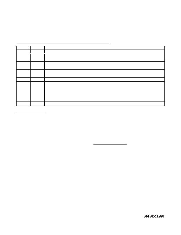
PIN NAME
FUNCTION
9
ONB ON Input. When low, the DC-DC is operational (Table 2).
10 PGND Power Ground
11
LX Inductor connection to the drain of P-channel synchronous rectifier and N-channel switch.
12 POUT
Boost Converter Power Output. POUT is the source of the P-channel synchronous-rectifier MOSFET
switch. Connect POUT to INL. Bypass POUT to PGND with a 100礔 capacitor.
13
INL
Linear Regulator Power Input. Source of PFET pass device connected between INL and OUTL. Connect
INL to POUT.
14 OUTL Linear Regulator Output. OUTL can source up to 500mA. Bypass OUTL to GND with a 4.7礔 capacitor.
15 TRACK
Track-Mode Control Input for DC-DC Converter. In track mode, the boost converter output is sensed at
OUT and set to 0.5V above OUTL to improve efficiency. Set TRACK to OUT for track mode and to GND
for normal operation (Table 2).
16
ONL
Linear Regulator ON Input. Enables the linear regulator output when TRACK = LOW. ONA and ONB
determine the linear regulators output state when TRACK = HIGH.
EP Exposed Pad (TSSOP Only). Internally connected to GND and PGND. Connect to a large ground plane.
Pin Description (continued)
相關PDF資料 |
PDF描述 |
|---|---|
| MAX1989MUE+ | IC TEMP SENSOR REMOTE 16TSSOP |
| MAX31723MUA+ | IC THERMOMETER/STAT SPI-3W 8UMAX |
| MAX31826MUA+T | IC TEMP SENSOR DIGITAL 8UMAX |
| MAX4006EUT+T | IC CURRENT MONITOR 1% SOT23-6 |
| MAX4008EUT+T | IC CURRENT MONITOR 1% SOT23-6 |
相關代理商/技術參數 |
參數描述 |
|---|---|
| MAX1765EUE+ | 功能描述:直流/直流開關轉換器 800mA Step-Up w/500mA Linear Reg RoHS:否 制造商:STMicroelectronics 最大輸入電壓:4.5 V 開關頻率:1.5 MHz 輸出電壓:4.6 V 輸出電流:250 mA 輸出端數量:2 最大工作溫度:+ 85 C 安裝風格:SMD/SMT |
| MAX1765EUE+T | 功能描述:直流/直流開關轉換器 800mA Step-Up w/500mA Linear Reg RoHS:否 制造商:STMicroelectronics 最大輸入電壓:4.5 V 開關頻率:1.5 MHz 輸出電壓:4.6 V 輸出電流:250 mA 輸出端數量:2 最大工作溫度:+ 85 C 安裝風格:SMD/SMT |
| MAX1765EUE-T | 功能描述:直流/直流開關轉換器 800mA Step-Up w/500mA Linear Reg RoHS:否 制造商:STMicroelectronics 最大輸入電壓:4.5 V 開關頻率:1.5 MHz 輸出電壓:4.6 V 輸出電流:250 mA 輸出端數量:2 最大工作溫度:+ 85 C 安裝風格:SMD/SMT |
| MAX1765EVKIT | 功能描述:直流/直流開關轉換器 Evaluation Kit for the MAX1765 RoHS:否 制造商:STMicroelectronics 最大輸入電壓:4.5 V 開關頻率:1.5 MHz 輸出電壓:4.6 V 輸出電流:250 mA 輸出端數量:2 最大工作溫度:+ 85 C 安裝風格:SMD/SMT |
| MAX176ACPA | 功能描述:模數轉換器 - ADC Integrated Circuits (ICs) RoHS:否 制造商:Texas Instruments 通道數量:2 結構:Sigma-Delta 轉換速率:125 SPs to 8 KSPs 分辨率:24 bit 輸入類型:Differential 信噪比:107 dB 接口類型:SPI 工作電源電壓:1.7 V to 3.6 V, 2.7 V to 5.25 V 最大工作溫度:+ 85 C 安裝風格:SMD/SMT 封裝 / 箱體:VQFN-32 |
發布緊急采購,3分鐘左右您將得到回復。