- 您現在的位置:買賣IC網 > PDF目錄16785 > MAX9737EVKIT+ (Maxim Integrated Products)KIT EVAL FOR MAX9737 PDF資料下載
參數資料
| 型號: | MAX9737EVKIT+ |
| 廠商: | Maxim Integrated Products |
| 文件頁數: | 11/13頁 |
| 文件大小: | 0K |
| 描述: | KIT EVAL FOR MAX9737 |
| 產品培訓模塊: | Lead (SnPb) Finish for COTS Obsolescence Mitigation Program |
| 標準包裝: | 1 |
| 放大器類型: | D 類 |
| 輸出類型: | 1-通道(單聲道) |
| 在某負載時最大輸出功率 x 通道數量: | 13W x 1 @ 4 歐姆 |
| 電源電壓: | 8 V ~ 28 V |
| 工作溫度: | -40°C ~ 85°C |
| 板類型: | 完全填充 |
| 已用 IC / 零件: | MAX9737 |
| 已供物品: | 板 |
Detailed Description
The MAX9737 filterless, mono class D audio power
amplifier offers Class AB audio performance and Class
D efficiency with minimal board space. The device
operates from an 8V to 28V supply range.
The MAX9737 features filterless, spread-spectrum
modulation, externally set gain and a low-power shut-
down mode that reduces supply current to less than
1A. Comprehensive click-and-pop suppression and
precharge circuitry reduce noise into and out of shut-
down or mute within 10ms.
Spread-Spectrum Modulation
The MAX9737 features a unique spread-spectrum
switching modulation that flattens EMI wideband spec-
tral components, reducing radiated emissions from the
speaker and cables. The switching frequency of the
Class D amplifier varies randomly by ±4kHz around the
300kHz center frequency. Instead of a large amount of
spectral energy present at multiples of the switching
frequency, the energy is spread over a bandwidth that
increases with frequency. Above a few MHz, the wide-
band spectrum looks like white noise for EMI purposes.
A proprietary amplifier topology ensures this white
noise does not corrupt the noise floor in the audio
bandwidth.
Efficiency
The high efficiency of a Class D amplifier is due to the
output transistors acting as switches and therefore con-
sume negligible power. Power loss associated with the
Class D output stage is due to the MOSFET I2R losses,
switching losses, and quiescent current.
Although the theoretical best efficiency of a linear
amplifier is 78% at peak output power, under typical
music reproduction levels, the efficiency falls to below
40%. The MAX9737 exhibits > 80% efficiency under the
same conditions (Figure 1).
Shutdown
The MAX9737 features a shutdown mode that reduces
power consumption to less than 1A (typ), extending
battery life in portable applications. Drive
SHDN low to
place the device in low-power shutdown mode. In shut-
down mode, the outputs are high impedance and the
common-mode voltage at the output decays to zero.
MAX9737
Mono 7W Class D Amplifier
_______________________________________________________________________________________
7
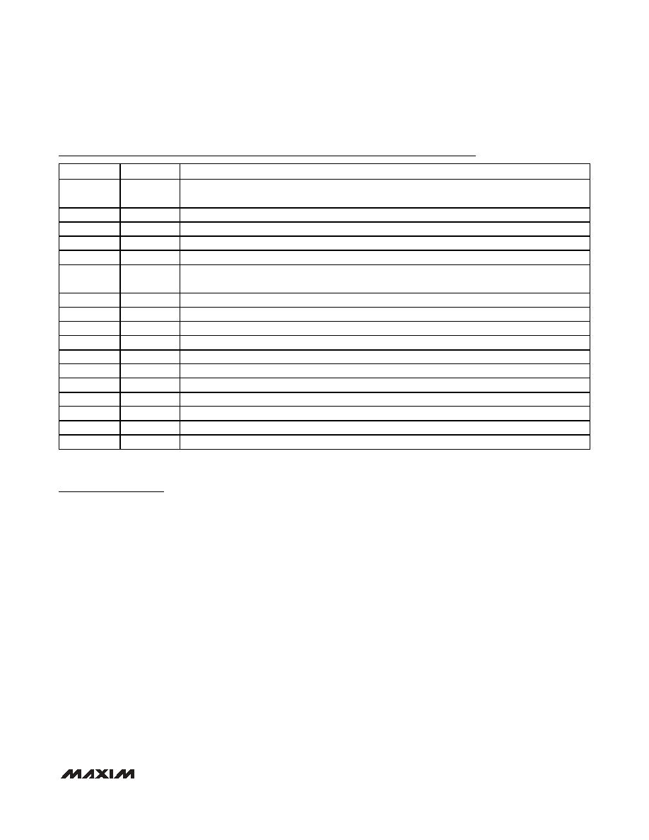
Pin Description
PIN
NAME
FUNCTION
1, 17, 18
PVDD
Power Supply. Bypass PVDD to PGND with a 1F capacitor connected to pin 1 and a 1F capacitor
connected to pins 17 and 18.
2
CHOLD
Charge-Pump Output. Connect a 1F capacitor to PVDD.
3, 10, 11
AGND
Analog Ground
4
MUTE
Mute Input. Drive MUTE low to place the device in mute mode.
5
SHDN
Shutdown Input. Drive SHDN low to place the part in shutdown mode.
6PC
Input Capacitor Precharge Connection. Connect between input resistor, RIN, and input coupling
capacitor, CIN.
7
IN
Op Amp Inverting Input.
8
PRE
Op Amp Output. PRE is the output of the input operational amplifier.
9
COM
Internal 2.0V Bias. Bypass COM to AGND with a 1F capacitor.
12
REG
Internal 4.2V Bias. Bypass REG to AGND with a 1F capacitor.
13, 14
VS
Internal 5.0V Bias. Bypass VS to AGND with a 1F capacitor.
15
C1N
Charge-Pump, Flying-Capacitor Negative Terminal. Connect C1N to C1P through a 0.1F capacitor.
16
C1P
Charge-Pump, Flying-Capacitor Positive Terminal. Connect C1P to C1N through a 0.1F capacitor.
19, 20
OUT-
Negative Speaker Output
21, 22
PGND
Power Ground
23, 24
OUT+
Positive Speaker Output
—
EP
Exposed Pad. Must be externally connected to PGND.
相關PDF資料 |
PDF描述 |
|---|---|
| H3BBS-2606G | IDC CABLE - HSR26S/AE26G/HSR26S |
| RNF-100-3/32-BN-STK | HEAT SHRINK TUBING |
| V300C15T75B3 | CONVERTER MOD DC/DC 15V 75W |
| 202G632-55-0 | BOOT MOLDED STRAIGHT |
| MC1403BDR2G | IC VREF SERIES PREC 2.5V 8-SOICN |
相關代理商/技術參數 |
參數描述 |
|---|---|
| MAX9737EVKIT+ | 功能描述:音頻 IC 開發工具 MAX9737 Eval Kit RoHS:否 制造商:Texas Instruments 產品:Evaluation Kits 類型:Audio Amplifiers 工具用于評估:TAS5614L 工作電源電壓:12 V to 38 V |
| MAX9738EVKIT+ | 功能描述:放大器 IC 開發工具 MAX9738 Eval Kit RoHS:否 制造商:International Rectifier 產品:Demonstration Boards 類型:Power Amplifiers 工具用于評估:IR4302 工作電源電壓:13 V to 23 V |
| MAX9738EWP+T | 制造商:Maxim Integrated Products 功能描述:16VP-P CLASS G AMPLIFIER WITH INVER - Tape and Reel |
| MAX9738EWP+TG45 | 功能描述:音頻放大器 16VP-P Class G Amplifier RoHS:否 制造商:STMicroelectronics 產品:General Purpose Audio Amplifiers 輸出類型:Digital 輸出功率: THD + 噪聲: 工作電源電壓:3.3 V 電源電流: 最大功率耗散: 最大工作溫度: 安裝風格:SMD/SMT 封裝 / 箱體:TQFP-64 封裝:Reel |
| MAX973C/D | 功能描述:校驗器 IC RoHS:否 制造商:STMicroelectronics 產品: 比較器類型: 通道數量: 輸出類型:Push-Pull 電源電壓-最大:5.5 V 電源電壓-最小:1.1 V 補償電壓(最大值):6 mV 電源電流(最大值):1350 nA 響應時間: 最大工作溫度:+ 125 C 安裝風格:SMD/SMT 封裝 / 箱體:SC-70-5 封裝:Reel |
發布緊急采購,3分鐘左右您將得到回復。