- 您現在的位置:買賣IC網 > PDF目錄371032 > MC34115DW (MOTOROLA INC) CONTINUOUSLY VARIABLE SLOPE DELTA MODULATOR/DEMODULATOR PDF資料下載
參數資料
| 型號: | MC34115DW |
| 廠商: | MOTOROLA INC |
| 元件分類: | 編解碼器 |
| 英文描述: | CONTINUOUSLY VARIABLE SLOPE DELTA MODULATOR/DEMODULATOR |
| 中文描述: | CVSD, CVSD CODEC, PDSO16 |
| 封裝: | PLASTIC, SO-16 |
| 文件頁數: | 12/16頁 |
| 文件大小: | 359K |
| 代理商: | MC34115DW |
MC34115
12
MOTOROLA ANALOG IC DEVICE DATA
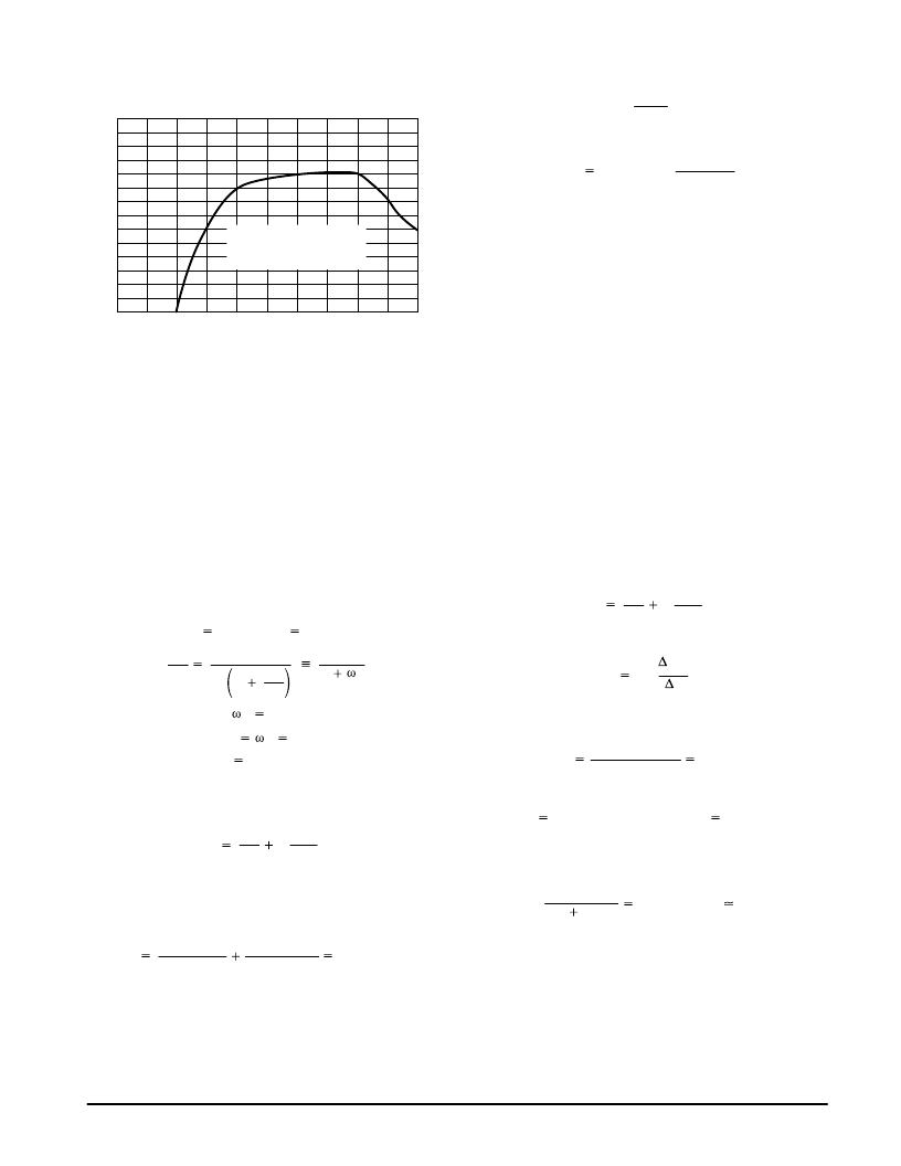
15
10
5.0
10
0
–10
–20
–30
–40
S
INPUT LEVEL (dB) RELATIVE TO SLOPE OVERLOAD
Clock Rate = 16 kHz
Test Tone = 1.0 kHz Sine Wave
Noise Weighting C Message
Figure 16. Signal–to–Noise Performance with
Single Integration, Single–Pole and
Companding at 16 k Bits (Typical)
Selection of Loop Gain
The gain of the circuit in Figure 15 is set by resistor Rx. Rx
must be selected to provide the proper integrator step size for
high level signals such that the companding ratio does not
exceed about 25%. The companding ratio is the active low
duty cycle of the coincidence output on Pin 11 of the codec
circuit. Thus, the system gain is dependent on:
1. The maximum level and frequency of the input signal.
2. The transfer function of the integration filter.
For voice codecs the typical input signal is taken to be a
sine wave at 1.0 kHz of 0 dBmo level. In practice, the useful
dynamic range extends about 6.0 dB above the design level.
In any system the companding ratio should not exceed 30%.
To calculate the required step size current, we must
describe the transfer characteristics of the integration filter. In
the basic circuit of Figure 15, a single–pole of 160 Hz is used.
R1
10 k
, C1
VO
Ii
C
S
RC
0.1
μ
F
1
1
K
S
o
o
2
π
f
103
o
2
π
f
f
159.2 Hz
Note that the integration filter produces a single–pole
response from 300 to 3.0 kHz. The current required to move
the integrator output a specific voltage from zero is simply:
VO
R
Now a 0 dBmo sine wave has a peak value of 1.0954 V. In
1/8 of a cycle of a sine wave centered around the zero
crossing, the sine wave changes by approximately its peak
value. The CVSD step should trace that change. The
required current for a 0 dBm 1.0 kHz sine wave is:
1.1 V
* 2 (10 k
)
0.125 ms
Ii
C
dVO
dt
Ii
0.1
μ
F (1.1)
0.935 mA
* The maximum voltage across R when maximum slew is
required is:
1.1 V
2
Now the voltage range of the syllabic filter is the power
supply voltage, thus:
Rx
0.25 (VCC)
1
0.935 mA
A similar procedure can be followed to establish the proper
gain for any input level and integration filter type.
Minimum Step Size
The final parameter to be selected for the simple codec in
Figure 15 is idle channel step size. With no input signal, the
digital output becomes a one–zero alternating pattern and
the analog output becomes a small triangle wave.
Mismatches of internal currents and offsets limit the minimum
step size which will produce a perfect idle channel pattern.
The MC34115 is tested to ensure that a 20 mVpp minimum
step size at 16 kHz will attain a proper idle channel. The idle
channel step size must be twice the specified total loop offset
if a one–zero idle pattern is desired. In some applications a
much smaller minimum step size (e.g., 0.1 mV) can produce
quiet performance without providing a 1 – 0 pattern.
To set the idle channel step size, the value of Rmin must be
selected. With no input signal, the slope control algorithm is
inactive. A long series of ones or zeros never occurs. Thus,
the voltage across the syllabic filter capacitor (CS) would
decay to zero. However, the voltage divider of RS and Rmin
(see Figure 15) sets the minimum allowed voltage across the
syllabic filter capacitor. That voltage must produce the
desired ramps at the analog output. Again we write the filter
input current equation:
VO
R
For values of VO near VCC/2 the VO/R term is negligible;
thus:
Ii
C
dVO
dt
Ii
CS
VO
T
where
T is the clock period and
VO is the desired
peak–to–peak value of the idle output. For a 16 k bit system
using the circuit in Figure 15:
0.1
μ
F 20 mV
62.5
μ
s
The voltage on CS which produces a 32
μ
A current is
determined by the value of Rx.
IiRx
In Figure 15 RS is 18 k
. That selection is discussed with
the syllabic filter considerations. The voltage divider of RS
and Rmin must produce an output of 41.6 mV.
RS
RS
Having established these three parameters – clock rate,
loop gain and minimum step size – the encoder circuit in
Figure 15 will function at near optimum performance for input
levels around 0 dBm.
Ii
32
μ
A
VSmin; for 32
μ
A, VSmin
41.6 mV
VCC
Rmin
VSmin Rmin
2.4 M
相關PDF資料 |
PDF描述 |
|---|---|
| MC34117D | ECONOLINE: RSZ/P - 1kVDC |
| MC34117 | Telephone tone ringer |
| MC34117P | Telephone tone ringer |
| MC34118 | ECONOLINE: RSZ/P - 1kVDC |
| MC34118DW | VOICE SWITCHED SPEAKERPHONE CIRCUIT |
相關代理商/技術參數 |
參數描述 |
|---|---|
| MC34115P | 制造商:MOTOROLA 制造商全稱:Motorola, Inc 功能描述:CONTINUOUSLY VARIABLE SLOPE DELTA MODULATOR/DEMODULATOR |
| MC34117 | 制造商:SPC Multicomp 功能描述:AXIAL FAN 17MM 3VDC 制造商:SPC Multicomp 功能描述:AXIAL FAN, 17MM, 3VDC 制造商:SPC Multicomp 功能描述:AXIAL FAN, 17MM, 3VDC; Frame Dimensions:17mm x 17mm x 3mm; Supply Voltage:3VDC; Current Rating:37mA; Flow Rate - Imperial:0.5cu.ft/min; Flow Rate - Metric:6.17l/min; Noise Rating:32.8dBA; Bearing Type:Vapo; Current Rating:39mA ;RoHS Compliant: Yes 制造商:SPC Multicomp 功能描述:AXIAL FAN, 17MM, 3VDC; Frame Dimensions:17mm x 17mm x 3mm; Supply Voltage:3VDC; Current Rating:37mA; Flow Rate - Imperial:0.5cu.ft/min; Flow Rate - Metric:6.17l/min; Noise Rating:32.8dBA; Bearing Type:Vapo; Series:-; Current Type:DC ;RoHS Compliant: Yes |
| MC34117D | 制造商:MOTOROLA 制造商全稱:Motorola, Inc 功能描述:Telephone tone ringer |
| MC34117P | 制造商:MOTOROLA 制造商全稱:Motorola, Inc 功能描述:Telephone tone ringer |
| MC34118 | 制造商:FREESCALE 制造商全稱:Freescale Semiconductor, Inc 功能描述:Specifications and Applications Information |
發布緊急采購,3分鐘左右您將得到回復。