- 您現在的位置:買賣IC網 > PDF目錄371083 > MCM62110 (Motorola, Inc.) 32K x 9 Bit Synchronous Dual I/O or Separate I/O Fast Static RAM with Parity Checker PDF資料下載
參數資料
| 型號: | MCM62110 |
| 廠商: | Motorola, Inc. |
| 英文描述: | 32K x 9 Bit Synchronous Dual I/O or Separate I/O Fast Static RAM with Parity Checker |
| 中文描述: | 32K的× 9位同步雙I / O或具有奇偶校驗檢查分離I / O快速靜態存儲器 |
| 文件頁數: | 2/12頁 |
| 文件大小: | 206K |
| 代理商: | MCM62110 |
MCM62110
2
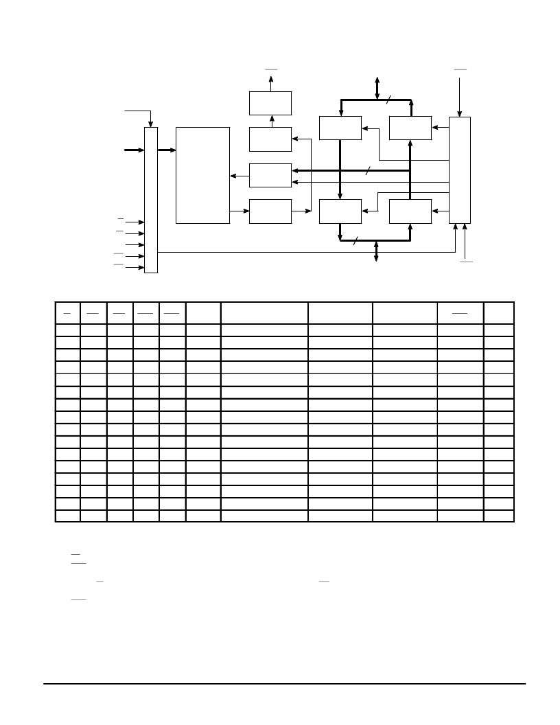
MOTOROLA FAST SRAM
BLOCK DIAGRAM
K
9
9
9
R
C
WRITE
DRIVER
A0 – A14
W
E1
E2
PIE
SIE
DPE
POE
SOE
32K
×
9 ARRAY
DATA
REGISTER
DATA
REGISTER
DATA
REGISTER
DATA
LATCH
DATA
LATCH
SENSE
AMPLIFIER
PARITY
CHECK
SDQ0 – SDQ7, SDQP
PDQ0 – PDQ7, PDQP
FUNCTIONAL TRUTH TABLE
(See Notes 1 and 2)
W
PIE
SIE
POE
SOE
Mode
Memory Subsystem
Cycle
PDQ0 – PDQ7,
PDQP Output
SDQ0 – SDQ7,
SDQP Output
DPE
Notes
1
1
1
0
1
Read
Processor Read
Data Out
High–Z
Parity Out
3, 4
1
1
1
1
0
Read
Copy Back
High–Z
Data Out
Parity Out
3, 4
1
1
1
0
0
Read
Dual Bus Read
Data Out
Data Out
Parity Out
3, 4
1
X
X
1
1
Read
NOP
High–Z
High–Z
1
X
0
0
X
X
N/A
NOP
High–Z
High–Z
1
2, 5
0
0
1
1
1
Write
Processor Write Hit
Data In
High–Z
1
2, 6
0
1
0
1
1
Write
Allocate
High–Z
Data In
1
2
0
0
1
1
0
Write
Write Through
Data In
Stream Data
1
2, 7
0
1
0
0
1
Write
Allocate With Stream
Stream Data
Data In
1
2, 7
1
0
1
1
0
N/A
Cache Inhibit Write
Data In
Stream Data
1
2, 7
1
1
0
0
1
N/A
Cache Inhibit Read
Stream Data
Data In
1
2, 7
0
1
1
X
X
N/A
NOP
High–Z
High–Z
1
5
X
0
1
0
0
N/A
Invalid
Data In
Stream
1
2, 8
X
0
1
0
1
N/A
Invalid
Data In
High–Z
1
2, 8
X
1
0
0
0
N/A
Invalid
Stream
Data In
1
2, 8
X
1
0
1
0
N/A
Invalid
High–Z
Data In
1
2, 8
NOTES:
1. A ‘0’ represents an input voltage
≤
VIL and a ‘1’ represents an input voltage
≥
VIH. All inputs must satisfy the specified setup and hold times
for the falling or rising edge of K. Some entries in this truth table represent latched values. This table assumes that the chip is selected (i.e.,
E1 = 0 and E2 = 1) and VCC current is equal to ICCA. If this is not true, the chip will be in standby mode, the VCC current will equal ISB1 or ISB2
DPE will default to 1 and all RAM outputs will be in High–Z. Other possible combinations of control inputs not covered by this note or the table
above are not supported and the RAM’s behavior is not specified.
2. If either IE signal is sampled low on the rising edge of clock, the corresponding OE is a don’t care, and the corresponding outputs are High–Z.
3. A read cycle is defined as a cycle where data is driven on the internal data bus by the RAM.
4. DPE is registered on the rising edge of K at the beginning of the following clock cycle
5. No RAM cycle is performed.
6. A write cycle is defined as a cycle where data is driven onto the internal data bus through one of the data I/O ports (PDQ0 – PDQ7 and PDQP
or SDQ0 – SDQ7 and SPDQ), and written into the RAM.
7. Data is driven on the internal data bus by one I/O port through its data input register and latched into the data output latch of the other I/O
port.
8. Data contention will occur.
相關PDF資料 |
PDF描述 |
|---|---|
| MCM62110FN15 | 32K x 9 Bit Synchronous Dual I/O or Separate I/O Fast Static RAM with Parity Checker |
| MCM62110FN17 | CAP CERM 10PF 200V NP0 RF 0603 |
| MCM62110FN20 | 32K x 9 Bit Synchronous Dual I/O or Separate I/O Fast Static RAM with Parity Checker |
| MCM6226BB | 128K x 8 Bit Static Random Access Memory |
| MCM6226BBXJ35R2 | 128K x 8 Bit Static Random Access Memory |
相關代理商/技術參數 |
參數描述 |
|---|---|
| MCM62110FN15 | 制造商:MOTOROLA 制造商全稱:Motorola, Inc 功能描述:32K x 9 Bit Synchronous Dual I/O or Separate I/O Fast Static RAM with Parity Checker |
| MCM62110FN17 | 制造商:MOTOROLA 制造商全稱:Motorola, Inc 功能描述:32K x 9 Bit Synchronous Dual I/O or Separate I/O Fast Static RAM with Parity Checker |
| MCM62110FN20 | 制造商:MOTOROLA 制造商全稱:Motorola, Inc 功能描述:32K x 9 Bit Synchronous Dual I/O or Separate I/O Fast Static RAM with Parity Checker |
| MCM6223YJ15 | 制造商:Motorola Inc 功能描述: |
| MCM6226BAXJ20 | 制造商:Motorola Inc 功能描述: |
發布緊急采購,3分鐘左右您將得到回復。