- 您現(xiàn)在的位置:買賣IC網(wǎng) > PDF目錄371087 > MCM63P531TQ7 (MOTOROLA INC) Replaced by PTH12000W : PDF資料下載
參數(shù)資料
| 型號: | MCM63P531TQ7 |
| 廠商: | MOTOROLA INC |
| 元件分類: | DRAM |
| 英文描述: | Replaced by PTH12000W : |
| 中文描述: | 32K X 32 CACHE SRAM, 7 ns, PQFP100 |
| 封裝: | TQFP-100 |
| 文件頁數(shù): | 17/27頁 |
| 文件大小: | 328K |
| 代理商: | MCM63P531TQ7 |
第1頁第2頁第3頁第4頁第5頁第6頁第7頁第8頁第9頁第10頁第11頁第12頁第13頁第14頁第15頁第16頁當(dāng)前第17頁第18頁第19頁第20頁第21頁第22頁第23頁第24頁第25頁第26頁第27頁
MCM63P636
17
MOTOROLA FAST SRAM
FUNCTIONAL OPERATION
POWER UP AND INITIALIZATION
The RESET input is used to reset the SRAM internal logic
at power on. At power on, this pin is held low and then driven
high at some later time. Eight cycles after the RESET is as-
serted high, standard SRAM functionality may begin.
DATA STROBES
The data strobes STRBA, STRBA, STRBB, and STRBB
are driven by the SRAM to be used by the device receiving
the output data. The data strobes toggle only at the approxi-
mate center of each output data valid window such that the
external device can reliably latch in this data. Following a
burst read, the data strobes will be driven to High–Z.
WRITE CYCLES
The address is sampled on the first rising edge of clock of
each burst write sequence, and the write data is sampled on
the subsequent rising clock edges. During a burst write the
last, last two, or last three addresses may be blocked from
being written by asserting the W synchronous write pin high.
However, once W is asserted high, it must remain in this
state through the remainder of the burst write sequence. All
burst write (and masked write) sequences must be followed
by an inactive cycle to reset internal state machines.
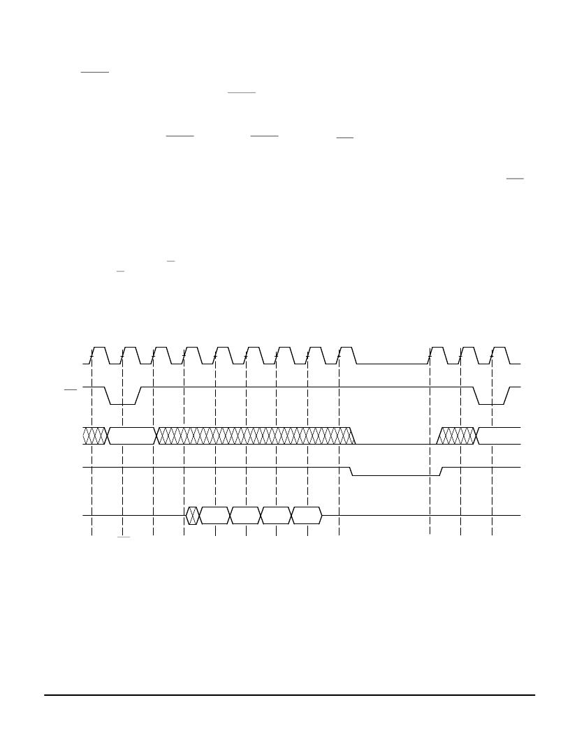
LOW POWER STOP–CLOCK OPERATION
In the stop–clock mode of operation, the SRAM will hold all
state and data values even though the clock is not running
(full static operation). The SRAM design allows the clock to
start with ADS, and stops the clock after the last write data is
latched, or the last read data is driven out.
When starting and stopping the clock, the initial clocks be-
ing driven may not meet the AC clock timing parametrics, but
will meet those parametrics at least two clocks prior to ADS
being asserted low.
To achieve the lowest power operation for all three stop
clock modes, stop read, stop write, and stop deselect:
Force the clock to a low state.
Force the control signals to an inactive state (this guar-
antees any potential source of noise on the clock input
will not start an unplanned on activity).
Force the address inputs to a low state (VIL), preferably
< 0.2 V.
VIL
K
ADS
SA
Din
Qout
A
B
VIH
VIL
VIL
HIGH–Z
HIGH–Z
STOP–CLOCK WITH READ TIMING
ADS
INITIATES
BURST READ
END
BURST
READ
K
CLOCK
STOP
STOP–CLOCK
LOW POWER
OPERATION
WAKE–UP/
INVALID
CLOCK
INVALID
CLOCK
FIRST
VALID
CLOCK
Q(A)
Q(A +1)
Q(A +2)
Q(A +3)
相關(guān)PDF資料 |
PDF描述 |
|---|---|
| MCM63P531TQ8 | 32K x 32 Bit Pipelined BurstRAM Synchronous Fast Static RAM |
| MCM63P531TQ9 | 32K x 32 Bit Pipelined BurstRAM Synchronous Fast Static RAM |
| MCM63P631 | 64K x 32 Bit Pipelined BurstRAM Synchronous Fast Static RAM |
| MCM63P631TQ7 | 64K x 32 Bit Pipelined BurstRAM Synchronous Fast Static RAM |
| MCM63P631TQ8 | 64K x 32 Bit Pipelined BurstRAM Synchronous Fast Static RAM |
相關(guān)代理商/技術(shù)參數(shù) |
參數(shù)描述 |
|---|---|
| MCM63P531TQ7R | 制造商:MOTOROLA 制造商全稱:Motorola, Inc 功能描述:32K x 32 Bit Pipelined BurstRAM Synchronous Fast Static RAM |
| MCM63P531TQ8 | 制造商:MOTOROLA 制造商全稱:Motorola, Inc 功能描述:32K x 32 Bit Pipelined BurstRAM Synchronous Fast Static RAM |
| MCM63P531TQ8R | 制造商:MOTOROLA 制造商全稱:Motorola, Inc 功能描述:32K x 32 Bit Pipelined BurstRAM Synchronous Fast Static RAM |
| MCM63P531TQ9 | 制造商:MOTOROLA 制造商全稱:Motorola, Inc 功能描述:32K x 32 Bit Pipelined BurstRAM Synchronous Fast Static RAM |
| MCM63P531TQ9R | 制造商:MOTOROLA 制造商全稱:Motorola, Inc 功能描述:32K x 32 Bit Pipelined BurstRAM Synchronous Fast Static RAM |
發(fā)布緊急采購,3分鐘左右您將得到回復(fù)。