- 您現在的位置:買賣IC網 > PDF目錄371092 > MCM69C433 (Motorola, Inc.) A Flexible Content-Addressable Memory (16K x 64 CAM)(1M內容可定址存儲器) PDF資料下載
參數資料
| 型號: | MCM69C433 |
| 廠商: | Motorola, Inc. |
| 英文描述: | A Flexible Content-Addressable Memory (16K x 64 CAM)(1M內容可定址存儲器) |
| 中文描述: | 一個靈活的內容尋址存儲器(16K的× 64 CAM)的(100萬內容可定址存儲器) |
| 文件頁數: | 11/22頁 |
| 文件大小: | 167K |
| 代理商: | MCM69C433 |
MCM69C433
SCM69C433
11
MOTOROLA FAST SRAM
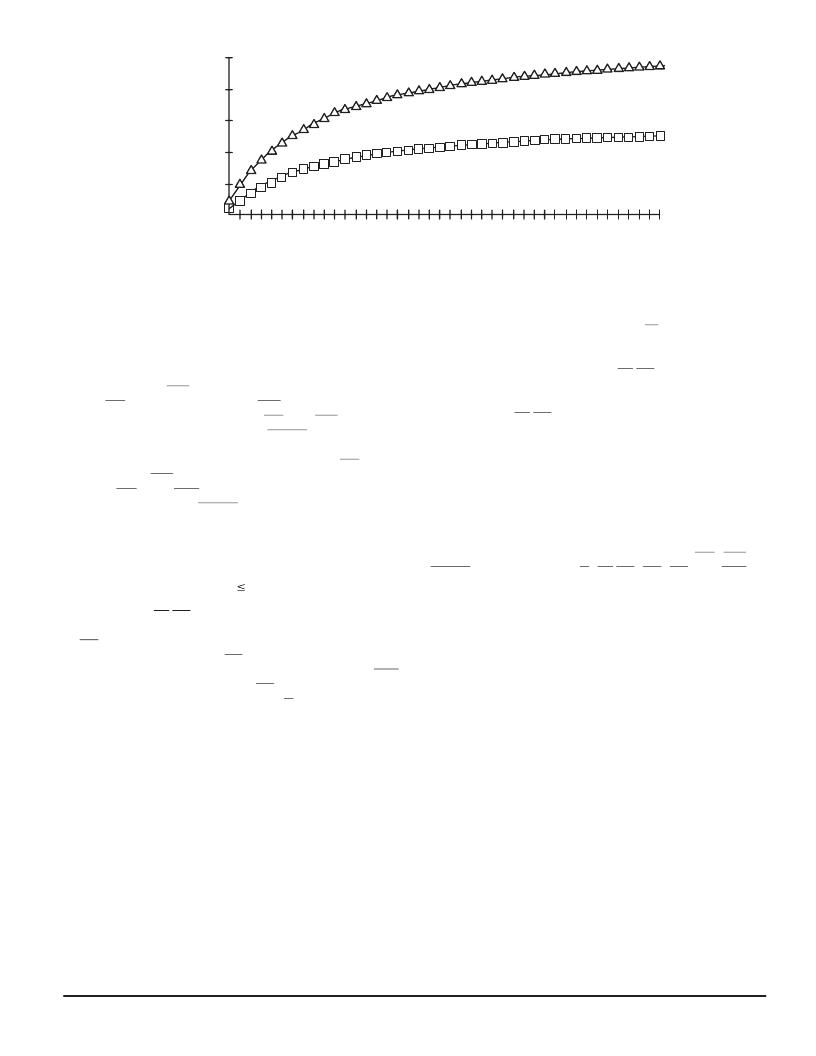
Figure 3. Connections per Second vs Match Cycle Time
MATCH CYCLE TIME IN CLOCK CYCLES
0
500
1,000
1,500
2,000
2,500
TYPICAL
WORST CASE
20
30
40
50
60
70
80
90
100
I
P
TIMING OVERVIEW
CONTROL PORT
The control port of the MCM69C433 is asynchronous.
Data transfers, both read and write, are initiated by the
assertion of the SEL signal. Address values should be valid
and WE should be high, when SEL is asserted to begin
a read cycle. All values (address, WE, and SEL) should be
held until the MCM69C433 asserts DTACK to signal the end
of the read cycle.
Address and data values should be valid and WE should
be low, when SEL is asserted to begin a write cycle. Address,
data, WE, and SEL values should be held until the
MCM69C433 asserts DTACK to signal the end of the write
cycle.
MATCH PORT
The MCM69C433’s match port is synchronous in opera-
tion. When the match width is
initiated by presenting the match data on MQ31 – MQ0 and
asserting the LH/SM signal with the appropriate setup time
relative to the rising edge of the clock. The assertion of the
MC output signifies the completion of the match cycle. If a
match has been found, the MS output is also asserted. If the
match is a virtual path circuit match in ATM mode, the VPC
output will be asserted with the MS output. Output data, if
any, is enabled by the assertion of the G input.
32 bits, a match cycle can be
If the match width is greater than 32 bits, the lower bits are
first latched into the MCM69C433 by the LL input. The match
cycle is then initiated as specified in the previous paragraph.
Two alternative timing diagrams are presented to describe
the Match Port timing. In the first, LH/SM must meet setup
and hold specs across two consecutive clock cycles, while
the MQ bus need only be valid for a single cycle. In the se-
cond diagram, LH/SM need only be asserted for a single
clock cycle, while the MQ bus must be held valid with
constant data across two clock cycles.
DEPTH EXPANSION
Multiple CAMs can be cascaded to increase the depth of
the match table. The hardware requirements are very
straightforward, as the following pins on each device are sim-
ply wired in parallel: A2 – A0, DQ15 – DQ0, WE, IRQ,
DTACK, MQ31 – MQ0, K, G, LH/SM, MC, MS, and VPC.
Four CAMs can be easily cascaded. Simulations show that
eight devices can be cascaded if care is taken to minimize
the length of the PC board traces connecting the CAMs.
The buffered–entry mode prevents multiple matching
entries in a single CAM. The check for value instruction
should be used to verify that multiple matching entries will
not result from a potential new entry. If a match is found in
CAM 1, for example, the new value should be placed in CAM 1,
where it will replace the existing entry.
相關PDF資料 |
PDF描述 |
|---|---|
| MCM69F536CTQ8.5 | 32K x 36 Bit Flow-Through BurstRAM Synchronous Fast Static RAM |
| MCM69F536CTQ9R | 32K x 36 Bit Flow-Through BurstRAM Synchronous Fast Static RAM |
| MCM69F536C | 32K x 36 Bit Flow-Through BurstRAM Synchronous Fast Static RAM |
| MCM69F536CTQ8.5R | 32K x 36 Bit Flow-Through BurstRAM Synchronous Fast Static RAM |
| MCM69F618CTQ9R | 64K x 18 Bit Flow-Through BurstRAM Synchronous Fast Static RAM |
相關代理商/技術參數 |
參數描述 |
|---|---|
| MCM69C433TQ15 | 制造商:MOTOROLA 制造商全稱:Motorola, Inc 功能描述:16K x 64 CAM |
| MCM69C433TQ15R | 制造商:MOTOROLA 制造商全稱:Motorola, Inc 功能描述:16K x 64 CAM |
| MCM69D536 | 制造商:MOTOROLA 制造商全稱:Motorola, Inc 功能描述:32K x 36 Bit Synchronous Dual I/O, Dual Address SRAM |
| MCM69D536TQ6 | 制造商:Motorola Inc 功能描述:Synchronous SRAM, 32K x 36, 176 Pin, Plastic, QFP |
| MCM69D536TQ6R | 制造商:MOTOROLA 制造商全稱:Motorola, Inc 功能描述:32K x 36 Bit Synchronous Dual I/O, Dual Address SRAM |
發布緊急采購,3分鐘左右您將得到回復。