- 您現在的位置:買賣IC網 > PDF目錄371121 > MMBF4392L (ON SEMICONDUCTOR) JFET Switching Transistors PDF資料下載
參數資料
| 型號: | MMBF4392L |
| 廠商: | ON SEMICONDUCTOR |
| 英文描述: | JFET Switching Transistors |
| 中文描述: | 結型場效應管開關晶體管 |
| 文件頁數: | 3/6頁 |
| 文件大小: | 139K |
| 代理商: | MMBF4392L |
3
Motorola Small–Signal Transistors, FETs and Diodes Device Data
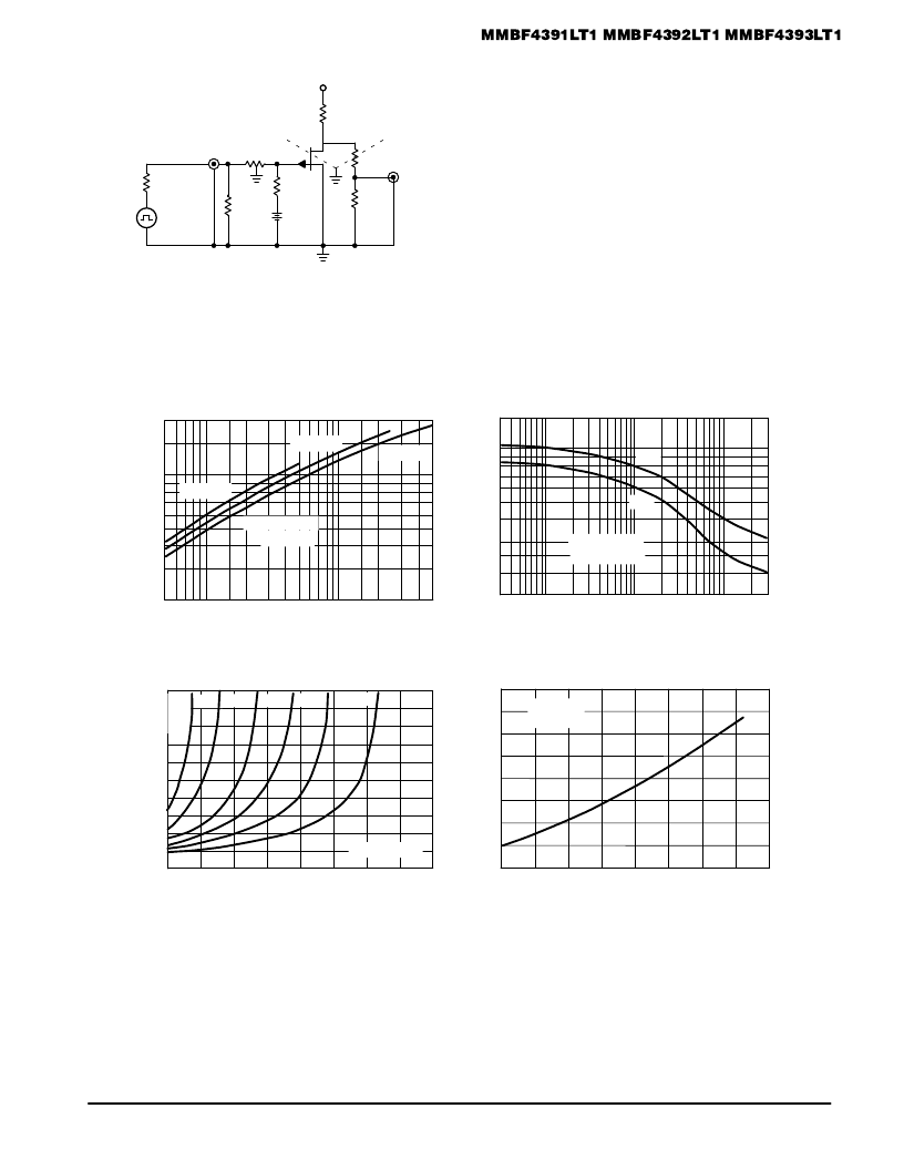
Figure 5. Switching Time Test Circuit
Figure 6. Typical Forward Transfer Admittance
Figure 7. Typical Capacitance
ID, DRAIN CURRENT (mA)
2.0
5.0
3.0
7.0
0.5
1.0
3.0
7.0
5.0
50
30
10
20
0.7
2.0
10
20
,
f
V
10
2.0
1.5
1.0
15
3.0
5.0
7.0
0.5
1.0
3.0
30
5.0
0.3
0.1
10
0.05
0.03
VR, REVERSE VOLTAGE (VOLTS)
C
Tchannel = 25
°
C
VDS = 15 V
Tchannel = 25
°
C
(Cds is negligible
Cgs
–VDD
VGG
RGG
RT
RGEN
50
VGEN
RK
RD
OUTPUT
INPUT
50
50
SET VDS(off) = –10 V
INPUT PULSE
tr
≤
0.25 ns
tf
≤
0.5 ns
PULSE WIDTH = 2.0
μ
s
DUTY CYCLE
≤
2.0%
RGG > RK
RD’ = RD(RT + 50)
RD + RT + 50
Figure 8. Effect of Gate–Source Voltage
on Drain–Source Resistance
80
120
160
200
50
1.0
3.0
170
5.0
20
–10
–40
2.0
80
140
–70
VGS, GATE–SOURCE VOLTAGE (VOLTS)
r
4.0
0
40
100 mA
125 mA
75 mA
50 mA
25 mA
IDSS
= 10
mA
Tchannel = 25
°
C
Figure 9. Effect of Temperature on Drain–Source
On–State Resistance
1.8
1.0
2.0
1.2
1.4
1.6
0.8
0.6
0.4
ID = 1.0 mA
VGS = 0
,
D
R
Tchannel, CHANNEL TEMPERATURE (
°
C)
Cgd
110
6.0
7.0
8.0
0
r
,
D
R
MMBF4393
MMBF4392
MMBF4391
NOTE 1
The switching characteristics shown above were measured using a test
circuit similar to Figure 5. At the beginning of the switching interval, the
gate voltage is at Gate Supply Voltage (–VGG). The Drain–Source Voltage
(VDS) is slightly lower than Drain Supply Voltage (VDD) due to the voltage
divider. Thus Reverse Transfer Capacitance (Crss) of Gate–Drain Capaci-
tance (Cgd) is charged to VGG + VDS.
During the turn–on interval, Gate–Source Capacitance (Cgs) discharges
through the series combination of RGen and RK. Cgd must discharge to
VDS(on) through RG and RK in series with the parallel combination of effec-
tive load impedance (R’D) and Drain–Source Resistance (rDS). During the
turn–off, this charge flow is reversed.
Predicting turn–on time is somewhat difficult as the channel resistance
rDS is a function of the gate–source voltage. While Cgs discharges, VGS
approaches zero and rDS decreases. Since Cgd discharges through rDS,
turn–on time is non–linear. During turn–off, the situation is reversed with
rDS increasing as Cgd charges.
The above switching curves show two impedance conditions; 1) RK is
equal to RD’ which simulates the switching behavior of cascaded stages
where the driving source impedance is normally the load impedance of the
previous stage, and 2) RK = 0 (low impedance) the driving source imped-
ance is that of the generator.
相關PDF資料 |
PDF描述 |
|---|---|
| MMBF4392LT1 | JFET Switching Transistors |
| MMBF4392L | RKZ Series - Econoline Unregulated DC-DC Converters; Input Voltage (Vdc): 05V; Output Voltage (Vdc): 05V; Power: 2W; High Isolation 2W Converter; Approved for Medical Applications; Custom Solutions Available; 3kVDC & 4kVDC Isolation Options; UL94V-0 Package Material; Optional Continuous Short Circuit Protected; Efficiency to 84% |
| MMBF4392LT1 | JFET Switching Transistors |
| MMBF4391 | RKZ Series - Econoline Unregulated DC-DC Converters; Input Voltage (Vdc): 05V; Output Voltage (Vdc): 05V; Power: 2W; High Isolation 2W Converter; Approved for Medical Applications; Custom Solutions Available; 3kVDC & 4kVDC Isolation Options; UL94V-0 Package Material; Optional Continuous Short Circuit Protected; Efficiency to 84% |
| MMBF5457LT1 | JFET - General Purpose Transistor |
相關代理商/技術參數 |
參數描述 |
|---|---|
| MMBF4392LT1 | 功能描述:JFET 30V 10mA RoHS:否 制造商:ON Semiconductor 晶體管極性:N-Channel 漏極電流(Vgs=0 時的 Idss):50 mA 漏源電壓 VDS:15 V 閘/源擊穿電壓: 漏極連續電流:50 mA 配置: 安裝風格: 封裝 / 箱體:SC-59 封裝:Reel |
| MMBF4392LT1G | 功能描述:JFET 30V 10mA RoHS:否 制造商:ON Semiconductor 晶體管極性:N-Channel 漏極電流(Vgs=0 時的 Idss):50 mA 漏源電壓 VDS:15 V 閘/源擊穿電壓: 漏極連續電流:50 mA 配置: 安裝風格: 封裝 / 箱體:SC-59 封裝:Reel |
| MMBF4392LT1G | 制造商:ON Semiconductor 功能描述:JFET |
| MMBF4393 | 功能描述:JFET N-Channel Switch RoHS:否 制造商:ON Semiconductor 晶體管極性:N-Channel 漏極電流(Vgs=0 時的 Idss):50 mA 漏源電壓 VDS:15 V 閘/源擊穿電壓: 漏極連續電流:50 mA 配置: 安裝風格: 封裝 / 箱體:SC-59 封裝:Reel |
| MMBF4393_Q | 功能描述:JFET N-Channel Switch RoHS:否 制造商:ON Semiconductor 晶體管極性:N-Channel 漏極電流(Vgs=0 時的 Idss):50 mA 漏源電壓 VDS:15 V 閘/源擊穿電壓: 漏極連續電流:50 mA 配置: 安裝風格: 封裝 / 箱體:SC-59 封裝:Reel |
發布緊急采購,3分鐘左右您將得到回復。