- 您現在的位置:買賣IC網 > PDF目錄371121 > MMBF4392L (ON SEMICONDUCTOR) JFET Switching Transistors PDF資料下載
參數資料
| 型號: | MMBF4392L |
| 廠商: | ON SEMICONDUCTOR |
| 英文描述: | JFET Switching Transistors |
| 中文描述: | 結型場效應管開關晶體管 |
| 文件頁數: | 5/6頁 |
| 文件大小: | 139K |
| 代理商: | MMBF4392L |
5
Motorola Small–Signal Transistors, FETs and Diodes Device Data
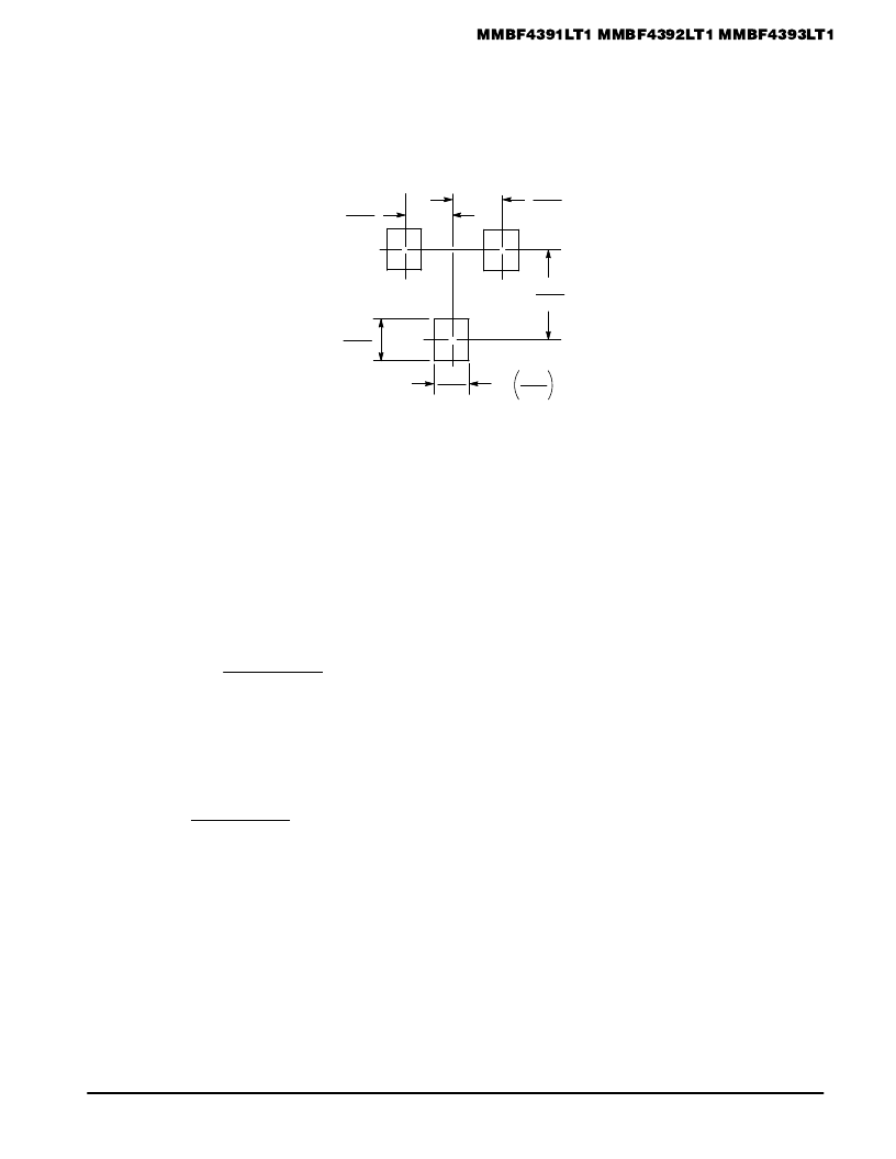
INFORMATION FOR USING THE SOT–23 SURFACE MOUNT PACKAGE
MINIMUM RECOMMENDED FOOTPRINT FOR SURFACE MOUNTED APPLICATIONS
Surface mount board layout is a critical portion of the total
design. The footprint for the semiconductor packages must
be the correct size to insure proper solder connection
interface between the board and the package. With the
correct pad geometry, the packages will self align when
subjected to a solder reflow process.
SOT–23
mm
inches
0.037
0.95
0.037
0.95
0.079
2.0
0.035
0.9
0.031
0.8
SOT–23 POWER DISSIPATION
The power dissipation of the SOT–23 is a function of the
pad size. This can vary from the minimum pad size for
soldering to a pad size given for maximum power dissipation.
Power dissipation for a surface mount device is determined
by TJ(max), the maximum rated junction temperature of the
die, R
θ
JA, the thermal resistance from the device junction to
ambient, and the operating temperature, TA. Using the
values provided on the data sheet for the SOT–23 package,
PD can be calculated as follows:
PD =
TJ(max) – TA
R
θ
JA
The values for the equation are found in the maximum
ratings table on the data sheet. Substituting these values into
the equation for an ambient temperature TA of 25
°
C, one can
calculate the power dissipation of the device which in this
case is 225 milliwatts.
PD =
150
°
C – 25
°
C
556
°
C/W
= 225 milliwatts
The 556
°
C/W for the SOT–23 package assumes the use
of the recommended footprint on a glass epoxy printed circuit
board to achieve a power dissipation of 225 milliwatts. There
are other alternatives to achieving higher power dissipation
from the SOT–23 package. Another alternative would be to
use a ceramic substrate or an aluminum core board such as
Thermal Clad
. Using a board material such as Thermal
Clad, an aluminum core board, the power dissipation can be
doubled using the same footprint.
SOLDERING PRECAUTIONS
The melting temperature of solder is higher than the rated
temperature of the device. When the entire device is heated
to a high temperature, failure to complete soldering within a
short time could result in device failure. Therefore, the
following items should always be observed in order to
minimize the thermal stress to which the devices are
subjected.
Always preheat the device.
The delta temperature between the preheat and
soldering should be 100
°
C or less.*
When preheating and soldering, the temperature of the
leads and the case must not exceed the maximum
temperature ratings as shown on the data sheet. When
using infrared heating with the reflow soldering method,
the difference shall be a maximum of 10
°
C.
The soldering temperature and time shall not exceed
260
°
C for more than 10 seconds.
When shifting from preheating to soldering, the
maximum temperature gradient shall be 5
°
C or less.
After soldering has been completed, the device should
be allowed to cool naturally for at least three minutes.
Gradual cooling should be used as the use of forced
cooling will increase the temperature gradient and result
in latent failure due to mechanical stress.
Mechanical stress or shock should not be applied during
cooling.
* Soldering a device without preheating can cause excessive
thermal shock and stress which can result in damage to the
device.
相關PDF資料 |
PDF描述 |
|---|---|
| MMBF4392LT1 | JFET Switching Transistors |
| MMBF4392L | RKZ Series - Econoline Unregulated DC-DC Converters; Input Voltage (Vdc): 05V; Output Voltage (Vdc): 05V; Power: 2W; High Isolation 2W Converter; Approved for Medical Applications; Custom Solutions Available; 3kVDC & 4kVDC Isolation Options; UL94V-0 Package Material; Optional Continuous Short Circuit Protected; Efficiency to 84% |
| MMBF4392LT1 | JFET Switching Transistors |
| MMBF4391 | RKZ Series - Econoline Unregulated DC-DC Converters; Input Voltage (Vdc): 05V; Output Voltage (Vdc): 05V; Power: 2W; High Isolation 2W Converter; Approved for Medical Applications; Custom Solutions Available; 3kVDC & 4kVDC Isolation Options; UL94V-0 Package Material; Optional Continuous Short Circuit Protected; Efficiency to 84% |
| MMBF5457LT1 | JFET - General Purpose Transistor |
相關代理商/技術參數 |
參數描述 |
|---|---|
| MMBF4392LT1 | 功能描述:JFET 30V 10mA RoHS:否 制造商:ON Semiconductor 晶體管極性:N-Channel 漏極電流(Vgs=0 時的 Idss):50 mA 漏源電壓 VDS:15 V 閘/源擊穿電壓: 漏極連續電流:50 mA 配置: 安裝風格: 封裝 / 箱體:SC-59 封裝:Reel |
| MMBF4392LT1G | 功能描述:JFET 30V 10mA RoHS:否 制造商:ON Semiconductor 晶體管極性:N-Channel 漏極電流(Vgs=0 時的 Idss):50 mA 漏源電壓 VDS:15 V 閘/源擊穿電壓: 漏極連續電流:50 mA 配置: 安裝風格: 封裝 / 箱體:SC-59 封裝:Reel |
| MMBF4392LT1G | 制造商:ON Semiconductor 功能描述:JFET |
| MMBF4393 | 功能描述:JFET N-Channel Switch RoHS:否 制造商:ON Semiconductor 晶體管極性:N-Channel 漏極電流(Vgs=0 時的 Idss):50 mA 漏源電壓 VDS:15 V 閘/源擊穿電壓: 漏極連續電流:50 mA 配置: 安裝風格: 封裝 / 箱體:SC-59 封裝:Reel |
| MMBF4393_Q | 功能描述:JFET N-Channel Switch RoHS:否 制造商:ON Semiconductor 晶體管極性:N-Channel 漏極電流(Vgs=0 時的 Idss):50 mA 漏源電壓 VDS:15 V 閘/源擊穿電壓: 漏極連續電流:50 mA 配置: 安裝風格: 封裝 / 箱體:SC-59 封裝:Reel |
發布緊急采購,3分鐘左右您將得到回復。