- 您現在的位置:買賣IC網 > PDF目錄371125 > MMDF2N06V (MOTOROLA INC) DUAL TMOS MOSFET 3.3 AMPERES 60 VOLTS PDF資料下載
參數資料
| 型號: | MMDF2N06V |
| 廠商: | MOTOROLA INC |
| 元件分類: | 小信號晶體管 |
| 英文描述: | DUAL TMOS MOSFET 3.3 AMPERES 60 VOLTS |
| 中文描述: | 3300 mA, 60 V, 2 CHANNEL, N-CHANNEL, Si, SMALL SIGNAL, MOSFET |
| 封裝: | MINIATURE, CASE 751-05, SO-8 |
| 文件頁數: | 1/4頁 |
| 文件大小: | 113K |
| 代理商: | MMDF2N06V |
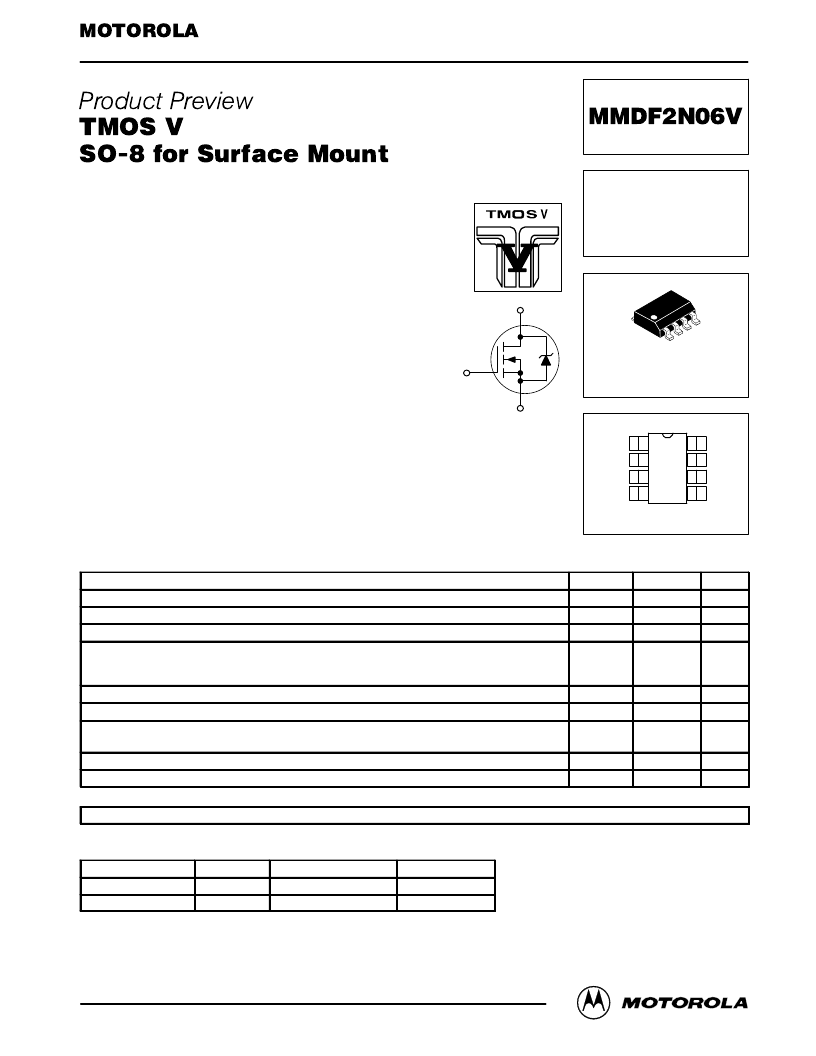
DUAL TMOS MOSFET
3.3 AMPERES
60 VOLTS
RDS(on) = 0.115 OHM
Source–1
Gate–1
Source–2
Gate–2
1
2
3
4
8
7
6
5
Top View
Drain–1
Drain–1
Drain–2
Drain–2
D
S
G
CASE 751–05, Style 11
SO–8
TM
1
Motorola TMOS Power MOSFET Transistor Device Data
N–Channel Enhancement–Mode Silicon Gate
TMOS V is a new technology designed to achieve an on–resis-
tance area product about one–half that of standard MOSFETs. This
new technology more than doubles the present cell density of our
50 and 60 volt TMOS devices. Just as with our TMOS E–FET
designs, TMOS V is designed to withstand high energy in the
avalanche and commutation modes. Designed for low voltage, high
speed switching applications in power supplies, converters and
power motor controls, these devices are particularly well suited for
bridge circuits where diode speed and commutating safe operating
areas are critical and offer additional safety margin against
unexpected voltage transients.
New Features of TMOS V
On–resistance Area Product about One–half that of Standard
MOSFETs with New Low Voltage, Low RDS(on) Technology
Faster Switching than E–FET Predecessors
Features Common to TMOS V and TMOS E–FETS
Avalanche Energy Specified
IDSS and VDS(on) Specified at Elevated Temperature
Static Parameters are the Same for both TMOS V and TMOS E–FET
Miniature SO–8 Surface Mount Package – Saves Board Space
Mounting Information for SO–8 Package Provided
MAXIMUM RATINGS
(TJ = 25
°
C unless otherwise noted)
Rating
Symbol
VDSS
VDGR
VGS
ID
ID
IDM
PD
TJ, Tstg
EAS
Value
60
60
±
20
3.3
0.5
9.9
2.0
–55 to 175
Unit
Vdc
Vdc
Vdc
Adc
Drain–to–Source Voltage
Drain–to–Gate Voltage, (RGS = 1 M
)
Gate–to–Source Voltage — Continuous
Drain Current — Continuous @ TA = 25
°
C
Drain Current
— Continuous @ TA = 100
°
C
Drain Current
— Single Pulse (tp
≤
10
μ
s)
Total Power Dissipation @ TA = 25
°
C (1)
Operating and Storage Temperature Range
Single Pulse Drain–to–Source Avalanche Energy — Starting TJ = 25
°
C
(VDD = 25 Vdc, VGS = 10 Vdc, Peak IL = 3.3 Apk, L = 10 mH, RG = 25
)
Thermal Resistance, Junction to Ambient (1)
Maximum Lead Temperature for Soldering Purposes, 0.0625
″
from case for 10 seconds
DEVICE MARKING
2N06V
(1) Mounted on G10/FR4 glass epoxy board using minimum recommended footprint.
ORDERING INFORMATION
Device
Reel Size
MMDF2N06V1
7
″
12mm embossed tape
MMDF2N06V2
13
″
12mm embossed tape
This document contains information on a new product. Specifications and information herein are subject to change without notice.
E–FET and TMOS V are trademarks of Motorola, Inc. TMOS is a registered trademark of Motorola, Inc.
Apk
W
°
C
mJ
54
R
θ
JA
TL
62.5
260
°
C/W
°
C
Tape Width
Quantity
500
2500
Order this document
by MMDF2N06V/D
SEMICONDUCTOR TECHNICAL DATA
相關PDF資料 |
PDF描述 |
|---|---|
| MMDF2P01HD | DUAL TMOS POWER FET 2.0 AMPERES 12 VOLTS |
| MMDF2P02E | DUAL TMOS MOSFET 2.5 AMPERES 25 VOLTS |
| MMDF2P02HD | DUAL TMOS POWER FET 2.0 AMPERES 20 VOLTS |
| MMDF3200Z | DUAL TMOS POWER MOSFET 11.5 AMPERES 20 VOLTS |
| MMDF3207 | DUAL TMOS POWER MOSFET 7.8 AMPERES 20 VOLTS |
相關代理商/技術參數 |
參數描述 |
|---|---|
| MMDF2N06VL | 制造商:MOTOROLA 制造商全稱:Motorola, Inc 功能描述:DUAL TMOS MOSFET 2.5 AMPERES 60 VOLTS |
| MMDF2P01HD | 制造商:MOTOROLA 制造商全稱:Motorola, Inc 功能描述:DUAL TMOS POWER FET 2.0 AMPERES 12 VOLTS |
| MMDF2P01HDR2 | 制造商:Rochester Electronics LLC 功能描述:- Bulk 制造商:ON Semiconductor 功能描述: |
| MMDF2P02E | 制造商:MOTOROLA 制造商全稱:Motorola, Inc 功能描述:DUAL TMOS MOSFET 2.5 AMPERES 25 VOLTS |
| MMDF2P02ER2 | 功能描述:MOSFET 25V 2A P-Channel RoHS:否 制造商:STMicroelectronics 晶體管極性:N-Channel 汲極/源極擊穿電壓:650 V 閘/源擊穿電壓:25 V 漏極連續電流:130 A 電阻汲極/源極 RDS(導通):0.014 Ohms 配置:Single 最大工作溫度: 安裝風格:Through Hole 封裝 / 箱體:Max247 封裝:Tube |
發布緊急采購,3分鐘左右您將得到回復。