- 您現在的位置:買賣IC網 > PDF目錄98048 > MUN2241T1G (ON SEMICONDUCTOR) 100 mA, 50 V, NPN, Si, SMALL SIGNAL TRANSISTOR PDF資料下載
參數資料
| 型號: | MUN2241T1G |
| 廠商: | ON SEMICONDUCTOR |
| 元件分類: | 小信號晶體管 |
| 英文描述: | 100 mA, 50 V, NPN, Si, SMALL SIGNAL TRANSISTOR |
| 封裝: | LEAD FREE, CASE 318D-04, SC-59, 3 PIN |
| 文件頁數: | 1/18頁 |
| 文件大小: | 160K |
| 代理商: | MUN2241T1G |
Semiconductor Components Industries, LLC, 2007
July, 2007 - Rev. 13
1
Publication Order Number:
MUN2211T1/D
MUN2211T1 Series
Preferred Devices
Bias Resistor Transistors
NPN Silicon Surface Mount Transistors
with Monolithic Bias Resistor Network
This new series of digital transistors is designed to replace a single
device and its external resistor bias network. The BRT (Bias Resistor
Transistor) contains a single transistor with a monolithic bias network
consisting of two resistors; a series base resistor and a base-emitter
resistor. The BRT eliminates these individual components by
integrating them into a single device. The use of a BRT can reduce
both system cost and board space. The device is housed in the
SC-59 package which is designed for low power surface
mount applications.
Features
Simplifies Circuit Design
Reduces Board Space
Reduces Component Count
Moisture Sensitivity Level: 1
ESD Rating - Human Body Model: Class 1
- Machine Model: Class B
The SC-59 Package can be Soldered Using Wave or Reflow
The Modified Gull-Winged Leads Absorb Thermal Stress During
Soldering Eliminating the Possibility of Damage to the Die
Pb-Free Packages are Available
MAXIMUM RATINGS (TA = 25°C unless otherwise noted)
Rating
Symbol
Value
Unit
Collector‐Base Voltage
VCBO
50
Vdc
Collector‐Emitter Voltage
VCEO
50
Vdc
Collector Current
IC
100
mAdc
THERMAL CHARACTERISTICS
Characteristic
Symbol
Max
Unit
Total Device Dissipation
TA = 25°C
Derate above 25
°C
PD
230 (Note 1)
338 (Note 2)
1.8 (Note 1)
2.7 (Note 2)
mW
°C/W
Thermal Resistance, Junction‐to‐Ambient
RqJA
540 (Note 1)
370 (Note 2)
°C/W
Thermal Resistance, Junction‐to‐Lead
RqJL
264 (Note 1)
287 (Note 2)
°C/W
Junction and Storage Temperature
Range
TJ, Tstg
-55 to +150
°C
Stresses exceeding Maximum Ratings may damage the device. Maximum
Ratings are stress ratings only. Functional operation above the Recommended
Operating Conditions is not implied. Extended exposure to stresses above the
Recommended Operating Conditions may affect device reliability.
1. FR-4 @ Minimum Pad.
2. FR-4 @ 1.0 x 1.0 inch Pad.
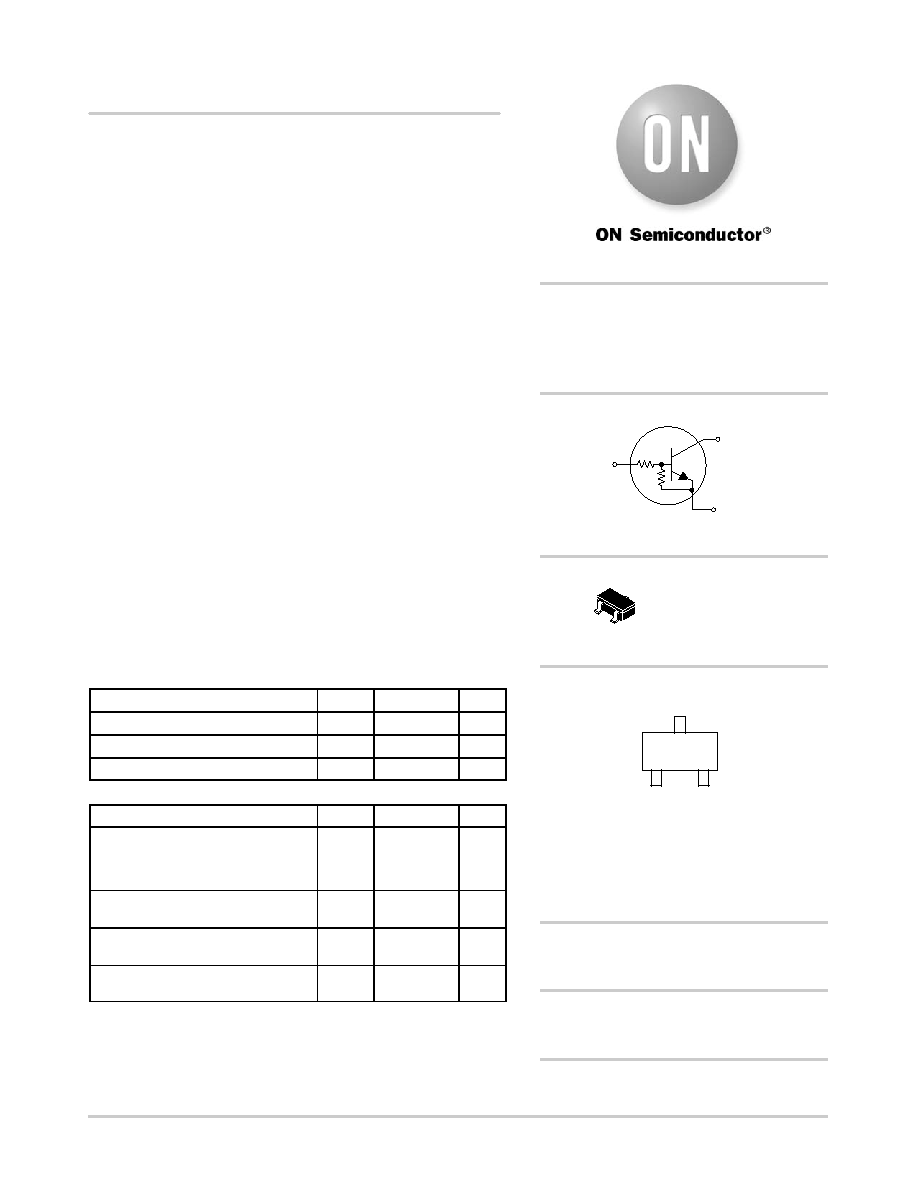
SC-59
CASE 318D
STYLE 1
Preferred devices are recommended choices for future use
and best overall value.
NPN SILICON
BIAS RESISTOR
TRANSISTORS
3
1
2
PIN 3
COLLECTOR
(OUTPUT)
PIN 1
EMITTER
(GROUND)
PIN 2
BASE
(INPUT)
R1
R2
MARKING DIAGRAM
DEVICE MARKING INFORMATION
See specific marking information in the Device Marking and
Resistor Values table on page 2 of this data sheet.
http://onsemi.com
See detailed ordering and shipping information in the table on
ORDERING INFORMATION
8x
= Device Code (Refer to page 2)
(Note: Microdot may be in either location)
8xM
G
*Date Code orientation may vary depending
upon manufacturing location.
1
相關PDF資料 |
PDF描述 |
|---|---|
| MUN2214T1G | 100 mA, 50 V, NPN, Si, SMALL SIGNAL TRANSISTOR |
| MUN5116T3 | 100 mA, 50 V, PNP, Si, SMALL SIGNAL TRANSISTOR |
| MUN5112T3 | 100 mA, 50 V, PNP, Si, SMALL SIGNAL TRANSISTOR |
| MUN5137T3 | 100 mA, 50 V, PNP, Si, SMALL SIGNAL TRANSISTOR |
| MUN5135T3 | 100 mA, 50 V, PNP, Si, SMALL SIGNAL TRANSISTOR |
相關代理商/技術參數 |
參數描述 |
|---|---|
| MUN22XXT1 | 制造商:ONSEMI 制造商全稱:ON Semiconductor 功能描述:NPN SILICON BIAS RESISTOR TRANSISTOR |
| MUN3222RT1 | 制造商:LRC 制造商全稱:Leshan Radio Company 功能描述:Bias Resistor Transistor |
| MUN511 | 制造商:ONSEMI 制造商全稱:ON Semiconductor 功能描述:Dual Bias Resistor Transistors |
| MUN5111 | 制造商:WEITRON 制造商全稱:Weitron Technology 功能描述:Bias Resistor Transistor PNP Silicon |
| MUN5111DW | 制造商:ONSEMI 制造商全稱:ON Semiconductor 功能描述:Dual Bias Resistor Transistors |
發布緊急采購,3分鐘左右您將得到回復。