- 您現(xiàn)在的位置:買賣IC網(wǎng) > PDF目錄361089 > NCN6004A (ON SEMICONDUCTOR) Dual SAM/SIM Interface Integrated Circuit PDF資料下載
參數(shù)資料
| 型號: | NCN6004A |
| 廠商: | ON SEMICONDUCTOR |
| 英文描述: | Dual SAM/SIM Interface Integrated Circuit |
| 中文描述: | 雙軟管/ SIM卡接口集成電路 |
| 文件頁數(shù): | 22/40頁 |
| 文件大小: | 329K |
| 代理商: | NCN6004A |
第1頁第2頁第3頁第4頁第5頁第6頁第7頁第8頁第9頁第10頁第11頁第12頁第13頁第14頁第15頁第16頁第17頁第18頁第19頁第20頁第21頁當前第22頁第23頁第24頁第25頁第26頁第27頁第28頁第29頁第30頁第31頁第32頁第33頁第34頁第35頁第36頁第37頁第38頁第39頁第40頁
NCN6004A
http://onsemi.com
22
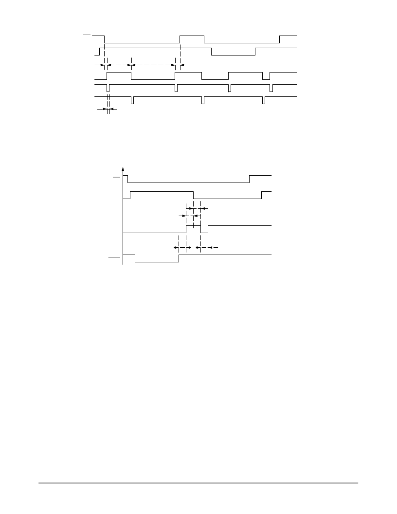
PWR_ON
tpwrhold
tpwrlow
CARD_SEL
SET
RESET
tpwrpre
tpwrset
tpwrp
NOTE:
tpwrset: This delay is necessary to latch–up the PWR_ON condition
and does not represent the CRD_VCC output voltage rise time.
tpwrlow: This delay includes the internal ISO7816-3 power down
sequence to make sure the DC/DC converter is fully deactivated.
Figure 13. Power On Sequence Timings
CS
PWR_ON
tpgmdly
CARD_SEL
tcseldly
tpwrw
Programming
Sequence
Chip Selected
tpwrhold
NOTE:
tpwrw: This delay represents the minimum pulse width needed
to write the PWR_ON status into the associated DC/DC latch
Figure 14. Power On and CARD_SEL Sequence Timings
CS
PGM
DC/DC CONVERTER
The power conversion is carried out either in step up or
step down mode. The operation is fully automatic and,
beside the output voltage programming, does not need any
further adjustments.
The simplified DC/DC converter, given in Figure 15, is
based on a full bridge structure capable to handle either step
up or step down power supply using an external inductor.
This structure brings the capability to operate from a wide
range of input voltage, while providing the accurate 1.80 V,
3.0 V or 5.0 V requested by the smart cards. Beside the
accuracy, the major aim of this structure is the high
efficiency necessary to save energy taken from the battery.
On the other hand, using two independent converters
provides a high flexibility and prevent a total system crash
in the event of a failure on one of the card connected to the
interface.
OPERATION
NOTE:
Described operation makes reference to
CARD_A and can be applied to CARD_B.
The system operates with a two cycles concept:
1. Cycle 1: Q15 and Q4 are switched ON and the
inductor L1 is charged by the energy supplied by
the external battery. During this phase, the pairs
Q1/Q16 and Q2/Q3 are switched OFF.
The current flowing into the two MOSFET Q1 and
Q4 is internally monitored and will be switched OFF
when the Ipeak value (depending upon the
programmed output voltage value) is reached. At
this point, Cycle 1 is completed and Cycle 2 takes
place. The ON time is a function of the battery
voltage and the value of the inductor network (L and
Zr) connected across pins 26/27 and 34/35.
A 4 s time out structure makes sure the system does
run in a continuous Cycle 1 loop.
2. Cycle 2: Q1 and Q16 are switched ON and the
energy stored into the inductor L1 is dumped into
the external load through Q16. During this phase,
the pair Q15/Q4 and the pair Q2/Q3 are switched
OFF.
The current flow period is constant (900 ns typical)
and Cycle 1 repeats after this time if the CRD_VCC
voltage is below the specified value.
相關(guān)PDF資料 |
PDF描述 |
|---|---|
| NCN6010DTBR2 | SIM Card Supply and Level Shifter |
| NCN6010 | SIM Card Supply and Level Shifter |
| NCN6010D | SIM Card Supply and Level Shifter |
| NCN6010DTB | SIM Card Supply and Level Shifter |
| NCP100(中文) | Sub 1V Precision Adjustable Shunt Regulator(基準電壓1V的精密可調(diào)旁路穩(wěn)壓器) |
相關(guān)代理商/技術(shù)參數(shù) |
參數(shù)描述 |
|---|---|
| NCN6004A/D | 制造商:ONSEMI 制造商全稱:ON Semiconductor 功能描述:Dual SAM/SIM Interface Integrated Circuit |
| NCN6004A_06 | 制造商:ONSEMI 制造商全稱:ON Semiconductor 功能描述:Dual SAM/SIM Interface Integrated Circuit |
| NCN6004AFTBR2 | 功能描述:輸入/輸出控制器接口集成電路 2.7V POS/ATM Smart RoHS:否 制造商:Silicon Labs 產(chǎn)品: 輸入/輸出端數(shù)量: 工作電源電壓: 最大工作溫度:+ 85 C 最小工作溫度:- 40 C 安裝風格:SMD/SMT 封裝 / 箱體:QFN-64 封裝:Tray |
| NCN6004AFTBR2G | 功能描述:輸入/輸出控制器接口集成電路 2.7V POS/ATM Smart Card Interface RoHS:否 制造商:Silicon Labs 產(chǎn)品: 輸入/輸出端數(shù)量: 工作電源電壓: 最大工作溫度:+ 85 C 最小工作溫度:- 40 C 安裝風格:SMD/SMT 封裝 / 箱體:QFN-64 封裝:Tray |
| NCN6010 | 制造商:ONSEMI 制造商全稱:ON Semiconductor 功能描述:SIM Card Supply and Level Shifter |
發(fā)布緊急采購,3分鐘左右您將得到回復(fù)。