- 您現在的位置:買賣IC網 > Datasheet目錄45 > NCP1605DR2G (ON Semiconductor)IC PFC CONTROLLER CCM/DCM 16SOIC Datasheet資料下載
參數資料
| 型號: | NCP1605DR2G |
| 廠商: | ON Semiconductor |
| 文件頁數: | 23/32頁 |
| 文件大小: | 745K |
| 描述: | IC PFC CONTROLLER CCM/DCM 16SOIC |
| 標準包裝: | 1 |
| 系列: | Soft-Skip™ |
| 模式: | 臨界傳導(CRM),間歇導電(DCM) |
| 頻率 - 開關: | 250kHz |
| 電流 - 啟動: | 12mA |
| 電源電壓: | 10 V ~ 20 V |
| 工作溫度: | 0°C ~ 125°C |
| 安裝類型: | 表面貼裝 |
| 封裝/外殼: | 16-SOIC(0.154",3.90mm 寬) |
| 供應商設備封裝: | 16-SOIC |
| 包裝: | 標準包裝 |
| 其它名稱: | NCP1605DR2GOSDKR |
第1頁第2頁第3頁第4頁第5頁第6頁第7頁第8頁第9頁第10頁第11頁第12頁第13頁第14頁第15頁第16頁第17頁第18頁第19頁第20頁第21頁第22頁當前第23頁第24頁第25頁第26頁第27頁第28頁第29頁第30頁第31頁第32頁
NCP1605, NCP1605A, NCP1605B
http://onsemi.com
23
3. Place a resistor R
DRV
between the drive pin and
Pin 6 to ease the circuit detection by creating
some overriding at the turn on instant. R
DRV
should be selected in the range of 3 times R
ZCD
.
For instance, if R
ZCD
is 6.2 kW, a 22 kW resistor
can be used for R
DRV
.
Overvoltage Protection
While PFC circuits often use one single pin for both the
Overvoltage Protection (OVP) and the feedback, the
NCP1605 dedicates one specific pin for the undervoltage
and overvoltage protections. The NCP1605 configuration
allows the implementation of two separate feedback
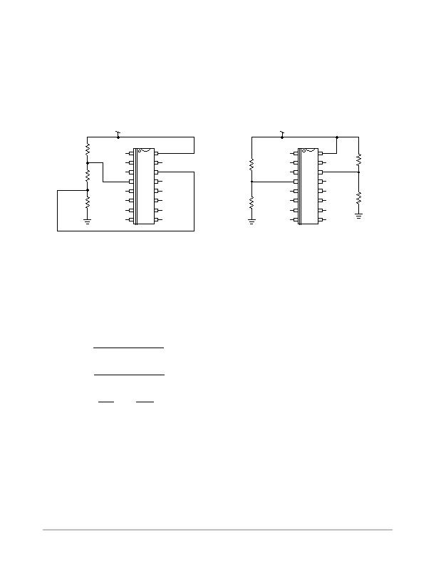
networks (see Figure 62):
One for regulation applied to Pin 4.
Another one for the OVP function.
Figure 61. Configuration with One Feedback
Network for Both OVP and Regulation
FB
HV
OVP
Vout (bulk voltage)
Figure 62. Configuration with Two Separate
Feedback Networks
1
2
3
4
13
16
14
15
5
6
7
8 9
12
10
11
R
out1
R
out3
R
out2
FB
HV
OVP
Vout (bulk voltage)
1
2
3
4
13
16
14
15
5
6
7
8 9
12
10
11
R
out1
R
out2
R
ovp1
R
ovp2
The double feedback configuration offers some
upgraded safety level as it protects the PFC stage even if
there is a failure of one of the two feedback arrangements.
However, if wished, one single feedback arrangement is
possible as portrayed by Figure 61. The regulation and
OVP blocks having the same reference voltage, the
resistance ratio Rout2 over Rout3 adjusts the OVP
threshold. More specifically,
The bulk regulation voltage is:
V
out
+
R
out1
) R
out2
) R
out3
R
out2
) R
out3
@ V
ref
The OVP level is:
V
ovp
+
R
out1
) R
out2
) R
out3
R
out2
@ V
ref
The ratio OVP level over regulation level is:
V
ovp
V
out
+ 1 )
R
out3
R
out2
For instance, (V
OVP
= 105% * V
out
) leads to the
following constraint: (R
out3
= 5% * R
out2
).
As soon and as long as the circuit detects that the output
voltage exceeds the OVP level, the power switch is turned
off to stop the power delivery.
Remark: Like in the NCP1601, the
V
TON
processing
circuit
is
informed
when there is an OVP condition, not
to overdimension V
TON
in that conditions. Otherwise, an
OVP sequence would be viewed as a deadtime phase by
the circuit and V
TON
would inappropriately increase to
compensate it (refer to Figure 56).
PfcOK / REF5V Signal
The NCP1605 can communicate with the downstream
converter. The signal
pfcOK/REF5V is high (5 V) when
the PFC stage is in normal operation (its output voltage is
stabilized at the nominal level) and low otherwise.
More specifically,
pfcOK/REF5V
is low:
" During the PFC stage startup, that is, as long as the
output voltage has not yet stabilized at the right level.
The startup phase is detected by the latch
L
STUP
of the
block diagram.
L
STUP
is set during each
off
phase so
that its output (
STUP
) is high when the circuit enters
an active phase. The latch is reset when the error
amplifier stops charging its output capacitor, that is,
when the output voltage of the PFC stage has reached its
desired regulation level. At that moment,
STUP
falls
down to indicate the end of the startup phase.
" In case of a condition preventing the circuit from
operating properly, i.e., during the V
CC
charge by the
high voltage startup current source, in a Brownout
case or when one of the following major faults turns
off the circuit:
Incorrect feeding of the circuit (
UVLO
high when
V
CC
<V
CC
OFF, V
CC
OFF equating 9 V typically).
Excessive die temperature detected by the thermal
shutdown.
Undervoltage Protection
Latched off of the circuit (when the
STDWN
pin,
V
Pin13
, exceeds 2.5 V).
相關PDF資料 |
PDF描述 |
|---|---|
| NCP1606BDR2G | IC POWER FACTOR CONTROLLER 8SOIC |
| NCP1607BDR2G | IC PFC CONTROLLER CRM 8SOIC |
| NCP1611BDR2G | IC PFC CTLR HE ENHANCED 8-SOIC |
| NCP1651DR2G | IC PFC CONTROLLER CCM/DCM 16SOIC |
| NCP1654BD133R2G | IC PFC CCM 133KHZ 8-SOIC |
相關代理商/技術參數 |
參數描述 |
|---|---|
| NCP1605FORWGEVB | 功能描述:電源管理IC開發工具 NCP1605 152 W FORWARD EVB RoHS:否 制造商:Maxim Integrated 產品:Evaluation Kits 類型:Battery Management 工具用于評估:MAX17710GB 輸入電壓: 輸出電壓:1.8 V |
| NCP1605LCDTVGEVB | 功能描述:BOARD EVAL NCP1605/1396 RoHS:是 類別:編程器,開發系統 >> 評估演示板和套件 系列:* 產品培訓模塊:Obsolescence Mitigation Program 標準包裝:1 系列:- 主要目的:電源管理,電池充電器 嵌入式:否 已用 IC / 零件:MAX8903A 主要屬性:1 芯鋰離子電池 次要屬性:狀態 LED 已供物品:板 |
| NCP1606ADR2G | 功能描述:功率因數校正 IC PWR FCTR CONTROLLER RoHS:否 制造商:Fairchild Semiconductor 開關頻率:300 KHz 最大功率耗散: 最大工作溫度:+ 125 C 安裝風格:SMD/SMT 封裝 / 箱體:SOIC-8 封裝:Reel |
| NCP1606APG | 功能描述:功率因數校正 IC LO CST PWR FCTR CONT RoHS:否 制造商:Fairchild Semiconductor 開關頻率:300 KHz 最大功率耗散: 最大工作溫度:+ 125 C 安裝風格:SMD/SMT 封裝 / 箱體:SOIC-8 封裝:Reel |
| NCP1606BDR2G | 功能描述:功率因數校正 IC PWR FCTR CONTROLLER RoHS:否 制造商:Fairchild Semiconductor 開關頻率:300 KHz 最大功率耗散: 最大工作溫度:+ 125 C 安裝風格:SMD/SMT 封裝 / 箱體:SOIC-8 封裝:Reel |
發布緊急采購,3分鐘左右您將得到回復。