- 您現在的位置:買賣IC網 > Datasheet目錄45 > NCP1651DR2G (ON Semiconductor)IC PFC CONTROLLER CCM/DCM 16SOIC Datasheet資料下載
參數資料
| 型號: | NCP1651DR2G |
| 廠商: | ON Semiconductor |
| 文件頁數: | 20/32頁 |
| 文件大小: | 779K |
| 描述: | IC PFC CONTROLLER CCM/DCM 16SOIC |
| 標準包裝: | 1 |
| 模式: | 連續導電(CCM),間歇導電(DCM) |
| 頻率 - 開關: | 25kHz ~ 250kHz |
| 電流 - 啟動: | 8.5mA |
| 電源電壓: | 10 V ~ 18 V |
| 工作溫度: | -40°C ~ 125°C |
| 安裝類型: | 表面貼裝 |
| 封裝/外殼: | 16-SOIC(0.154",3.90mm 寬) |
| 供應商設備封裝: | 16-SOIC |
| 包裝: | 標準包裝 |
| 其它名稱: | NCP1651DR2GOSDKR |
第1頁第2頁第3頁第4頁第5頁第6頁第7頁第8頁第9頁第10頁第11頁第12頁第13頁第14頁第15頁第16頁第17頁第18頁第19頁當前第20頁第21頁第22頁第23頁第24頁第25頁第26頁第27頁第28頁第29頁第30頁第31頁第32頁
NCP1651
http://onsemi.com
20
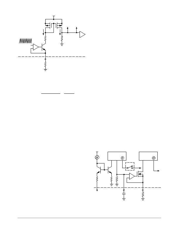
Figure 35. Ramp Compensation Circuit
--
+
Oscillator
--
+
16 k
AC Ref
Buffer
Current
Sense
Amp
PWM
Comparator
4
Ramp Compensation
R
RC
1.6i
i
The current mirror is designed with a 1:1.6 current ratio.
Therampsignalinjectedcanbecalculatedbythefollowing
formula:
V
ramp
=
1.6 Vosc
pk
16 k
R
RC
=
102,400
R
RC
(eq. 1)
Where:
V
ramp
= Peak injected current signal (4 V)
R
RC
= Ramp compensation resistor (k?
Oscillator
Theoscillatorgeneratesthesawtoothrampsignalthatsets
the switching frequency, as well as sets the gain for the
multipliers. Both the frequency and the peak- -to- -peak
amplitude are important parameters.
The oscillator uses a current source for charging the
capacitor on the C
T
pin. The charge rate is approximately
200 mA and is trimmed to maintain an accurate, repeatable
frequency. Discharge is accomplished by grounding the C
T
pin with a saturated transistor. A hysteretic comparator
monitorsthatrampsignalandisusedtoswitchbetweenthe
current source and discharge transistor. While the cap is
charging, the comparator has a reference voltage of
4.0 volts. When the ramp reaches that voltage, the
comparator switches from the charging circuit to the
dischargecircuit,anditsreferencechangesfrom4.0to~0.5
volts (overshoot and delays will allow the valley voltage to
reach 0 volts).
The relationship between the frequency and timing
capacitor is:
C
T
= 47,000f
Where C
T
is in pF and f is in kHz.
It is important not to load the capacitor on this pin, since
thiscouldaffecttheaccuracyofthefrequencyaswellasthat
ofthemultiplierswhichusetherampsignal.Anyuseofthis
signal should incorporate a high impedance buffer.
Due to the requiredaccuracy of the peakand valleyramp
voltages, the NCP1651 is not designed to be synchronized
to the frequency of another oscillator.
Average Current Compensation
The input signal to this amplifier is the input fullwave
rectified sinewave. The amplifier is a unity gain amplifier,
withavoltagedividerontheoutputthatattenuatesthesignal
by a factor of 0.75. This scaled down fullwave rectified
sinewave is summed with the low frequency current signal
out of the current sense amplifier.
The sum of these signals must equal the signal at the
non- -inverting input to the AC error amplifier, which is the
outputofthereferencemultiplier.Sincethereisahardlimit
of 4.5 volts at the non- -inverting input, the sum of the line
voltage plus the current cannot exceed this level.
A typical universal input design operates from 85 to
265vac,whichisarangeof3.1:1.TheoutputoftheCurrent
Compensationamplifierwillchangebythisamounttoallow
the maximum current to vary inversely to the line voltage.
AC Error Amplifier
The AC error amplifier is a transconductance amplifier.
Thisamplifierforcesasignalwhichisthesumofthecurrent
and input voltage to equal the AC reference signal fromthe
reference multiplier.
Transconductance amplifiers differ from voltage
amplifiers in that the output is a high impedance with a
controlled voltage- -to- -current gain. This amplifier has a
nominal gain of 100 umhos (or 0.0001 amps/volt). This
means that an input voltage differential of 10 mv would
cause the output current to change by 1.0 mA. Itsmaximum
output current is 30 mA.
Current Sense Amplifier
Thecurrentsenseamplifierisawidebandwidthamplifier
with a differential input. It consists of a differential input
stage, a high frequency current mirror (PWM output) and a
low frequency current mirror (AC error amp output).
Figure 36. Current Sense Amplifier
CURRENT
MIRROR
--
+
I
avg
AC
Error
Amp
i
2
i
2
I
avg fltr
CURRENT
MIRROR
i
1
i
1
i
1
PWM
3 k
30 k
3 k
6
7
I
S+
5
LEB
相關PDF資料 |
PDF描述 |
|---|---|
| NCP1654BD133R2G | IC PFC CCM 133KHZ 8-SOIC |
| NCP1927DR2G | IC CTLR PFC/FLYBACK 16-SOIC |
| NCP380HMU21AATBG | IC CURRENT LIMIT SWITCH 6-UDFN |
| NCT1008DMT3R2G | TMP DIO MON/SMBUS 4CH 8WDFN |
| NCT210RQR2G | IC TEMP SENSOR LOC/REM 16QSOP |
相關代理商/技術參數 |
參數描述 |
|---|---|
| NCP1652ADR2G | 功能描述:功率因數校正 IC ANA PFC CONTROLLER RoHS:否 制造商:Fairchild Semiconductor 開關頻率:300 KHz 最大功率耗散: 最大工作溫度:+ 125 C 安裝風格:SMD/SMT 封裝 / 箱體:SOIC-8 封裝:Reel |
| NCP1652DR2G | 功能描述:功率因數校正 IC ANA PFC CONTROLLER RoHS:否 制造商:Fairchild Semiconductor 開關頻率:300 KHz 最大功率耗散: 最大工作溫度:+ 125 C 安裝風格:SMD/SMT 封裝 / 箱體:SOIC-8 封裝:Reel |
| NCP1652DWR2G | 功能描述:功率因數校正 IC ANA PFC CONTROLLER RoHS:否 制造商:Fairchild Semiconductor 開關頻率:300 KHz 最大功率耗散: 最大工作溫度:+ 125 C 安裝風格:SMD/SMT 封裝 / 箱體:SOIC-8 封裝:Reel |
| NCP1652L48VGEVB | 功能描述:電源管理IC開發工具 100W PFC 48V FIXED VOLTAGE RoHS:否 制造商:Maxim Integrated 產品:Evaluation Kits 類型:Battery Management 工具用于評估:MAX17710GB 輸入電壓: 輸出電壓:1.8 V |
| NCP1653ADR2 | 功能描述:功率因數校正 IC Fixed Frequency RoHS:否 制造商:Fairchild Semiconductor 開關頻率:300 KHz 最大功率耗散: 最大工作溫度:+ 125 C 安裝風格:SMD/SMT 封裝 / 箱體:SOIC-8 封裝:Reel |
發布緊急采購,3分鐘左右您將得到回復。