- 您現(xiàn)在的位置:買賣IC網(wǎng) > PDF目錄382370 > PA7536T-15 ASIC PDF資料下載
參數(shù)資料
| 型號: | PA7536T-15 |
| 英文描述: | ASIC |
| 中文描述: | 專用集成電路 |
| 文件頁數(shù): | 9/10頁 |
| 文件大小: | 219K |
| 代理商: | PA7536T-15 |
9
04-02-052D
Commercial/Industrial
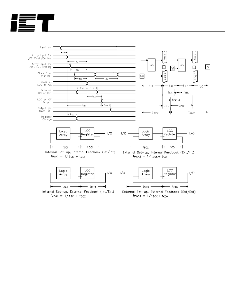
Figure 16. Sequential Timing
–
Waveforms and Block Diagram
Notes
1. Minimum DC input is -0.5V, however inputs may under-shoot to -2.0V
for periods less than 20ns.
2.Test points for Clock and V
CC
in t
R
,t
F
,t
CL
,t
CH
, and t
RESET
are referenced at
10% and 90% levels.
3. I/O pins are 0V or V
CC
.
4. Test one output at a time for a duration of less than 1 sec.
5. Capacitances are tested on a sample basis.
6. Test conditions assume: signal transition times of 5ns or less from the
10% and 90% points, timing reference levels of 1.5V (unless
otherwise specified).
7. t
OE
is measured from input transition to V
±0.1V (See test loads at
end of Section 6 for V
REF
value). t
OD
is measured from input transition
to V
OH
-0.1V or V
OL
+0.1V.
8.
“
System-clock
”
refers to pin 1 or pin 28 high speed clocks.
9. For T or JK registers in toggle (divide by 2) operation only.
10. For combinatorial and async-clock to LCC output delay.
11. ICC for a typical application: This parameter is tested with the device
programmed as a 10-bit D-type counter.
12. Test loads are specified in Section 5 of the Data Book.
13.
“
Async. Clock
”
refers to the clock from the Sum term (OR gate).
14. The
“
LCC
”
term indicates that the timing parameter is applied to the
LCC register. The
“
IOC
”
term indicates that the timing parameter is
applied to the IOC register. The
“
LCC/IOC
”
term indicates that the
timing parameter is applied to both the LCC and IOC registers. The
“
LCC/IOC/INC
”
term indicates that the timing parameter is applied to
the LCC,IOC, and INC registers.
15. This refers to the Sum-D gate routed to the IOC register for an
additional buried register.
16. The term
“
input
”
without any reference to another term refers to an
(external) input pin.
17. The parameter t
SPI
indicates that the PCLK signal to the IOC register
is always slower than the data from the pin or input by the absolute
value of (t
SK
-t
PK
-t
IA
). This means that no set-up time for the data
from the pin or input is required, i.e. the external data and clock can
be sent to the device simultaneously. Additionally, the data from the
pin must remain stable for t
HPI
time, i.e. to wait for the PCLK signal to
arrive at the IOC register.
18. Typical (typ) ICC is measured at T
A
= 25
°
C, freq = 25MHZ, V
CC
=
5V
相關(guān)PDF資料 |
PDF描述 |
|---|---|
| PA7536TI-15 | ASIC |
| PA7536J-15 | ASIC |
| PA7 | Analog IC |
| PAC21S07AS | Analog IC |
| PACK-1 | |
相關(guān)代理商/技術(shù)參數(shù) |
參數(shù)描述 |
|---|---|
| PA7536TI-15 | 制造商:未知廠家 制造商全稱:未知廠家 功能描述:ASIC |
| PA7540 | 制造商:ANACHIP 制造商全稱:Anachip Corp 功能描述:PA7540 PEEL Array? Programmable Electrically Erasable Logic Array |
| PA7540J-15 | 功能描述:EEPLD - 電子擦除可編程邏輯設(shè)備 2 INP 20 I/O 15ns RoHS:否 制造商:Atmel 邏輯系列:ATF16V8BQL 最大工作頻率:62 MHz 可編程輸入/輸出端數(shù)量:20 電源電流:20 mA 延遲時(shí)間:15 ns 每個(gè)宏指令的積項(xiàng)數(shù):8 電源電壓-最大:5.5 V 電源電壓-最小:4.5 V 大電池?cái)?shù)量:8 最小工作溫度:- 40 C 最大工作溫度:+ 85 C 安裝風(fēng)格:Through Hole 封裝 / 箱體:PDIP-20 |
| PA7540J-15L | 功能描述:EEPLD - 電子擦除可編程邏輯設(shè)備 2 INP 20 I/O 15ns RoHS:否 制造商:Atmel 邏輯系列:ATF16V8BQL 最大工作頻率:62 MHz 可編程輸入/輸出端數(shù)量:20 電源電流:20 mA 延遲時(shí)間:15 ns 每個(gè)宏指令的積項(xiàng)數(shù):8 電源電壓-最大:5.5 V 電源電壓-最小:4.5 V 大電池?cái)?shù)量:8 最小工作溫度:- 40 C 最大工作溫度:+ 85 C 安裝風(fēng)格:Through Hole 封裝 / 箱體:PDIP-20 |
| PA7540JI-15 | 功能描述:EEPLD - 電子擦除可編程邏輯設(shè)備 2 INP 20 I/O 15ns RoHS:否 制造商:Atmel 邏輯系列:ATF16V8BQL 最大工作頻率:62 MHz 可編程輸入/輸出端數(shù)量:20 電源電流:20 mA 延遲時(shí)間:15 ns 每個(gè)宏指令的積項(xiàng)數(shù):8 電源電壓-最大:5.5 V 電源電壓-最小:4.5 V 大電池?cái)?shù)量:8 最小工作溫度:- 40 C 最大工作溫度:+ 85 C 安裝風(fēng)格:Through Hole 封裝 / 箱體:PDIP-20 |
發(fā)布緊急采購,3分鐘左右您將得到回復(fù)。