- 您現在的位置:買賣IC網 > PDF目錄382378 > PCA9515 (NXP Semiconductors N.V.) I2C-bus repeater PDF資料下載
參數資料
| 型號: | PCA9515 |
| 廠商: | NXP Semiconductors N.V. |
| 英文描述: | I2C-bus repeater |
| 中文描述: | I2C總線中繼器 |
| 文件頁數: | 2/11頁 |
| 文件大小: | 128K |
| 代理商: | PCA9515 |
Philips Semiconductors
Product data sheet
PCA9515
I
2
C-bus repeater
2
2004 Jun 24
DESCRIPTION
The PCA9515 is a BiCMOS integrated circuit intended for
application in I
2
C and SMBus systems.
While retaining all the operating modes and features of the I
2
C
system it permits extension of the I
2
C-bus by buffering both the data
(SDA) and the clock (SCL) lines, thus enabling two buses of 400 pF.
The I
2
C-bus capacitance limit of 400 pF restricts the number of
devices and bus length. Using the PCA9515 enables the system
designer to isolate two halves of a bus, thus more devices or longer
length can be accommodated. It can also be used to run two buses,
one at 5 V and the other at 3.3 V or a 400 kHz and 100 kHz bus,
where the 100 kHz bus is isolated when 400 kHz operation of the
other is required.
Two or more PCA9515s cannot be put in series.
The PCA9515
design does not allow this configuration. Since there is no direction
pin, slightly different “legal” low voltage levels are used to avoid
lock-up conditions between the input and the output. A “regular low”
applied at the input of a PCA9515 will be propagated as a “buffered
low” with a slightly higher value. When this “buffered low” is applied
to another PCA9515, PCA9516, or PCA9518 in series, the second
PCA9515, PCA9516, or PCA9518 will not recognize it as a “regular
low” and will not propagate it as a “buffered low” again. The
PCA9511/9513/9514 and PCA9512 cannot be used in series with
the PCA9515, PCA9516, or PCA9518 but can be used in series with
themselves since they use shifting instead of static offsets to avoid
lock-up conditions.
FEATURES
2 channel, bi-directional buffer
I
2
C-bus and SMBus compatible
Active-HIGH repeater enable input
Open-drain input/outputs
Lock-up free operation
Supports arbitration and clock stretching across the repeater
Accommodates standard mode and fast mode I
2
C devices and
multiple masters
Powered-off high impedance I
2
C pins
Operating supply voltage range of 3.0 V to 3.6 V
5.5 V tolerant I
2
C and enable pins
0 to 400 kHz clock frequency
1
ESD protection exceeds 2000 V HBM per JESD22-A114,
200 V MM per JESD22-A115, and 1000 V CDM per
JESD22-C101.
Latch-up testing is done to JEDEC Standard JESD78 which
exceeds 100 mA.
Package offerings: SO and TSSOP
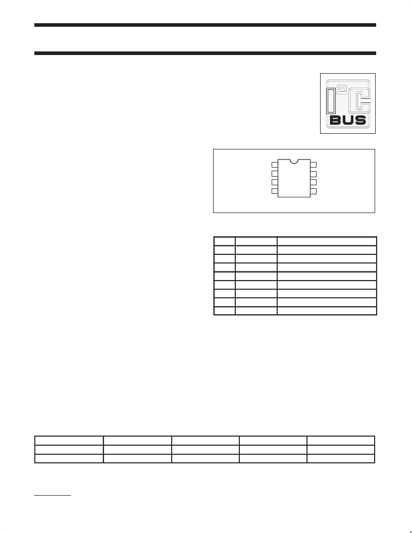
PIN CONFIGURATION
1
2
3
4
n.c.
GND
SDA0
SCL1
SDA1
EN
5
6
7
8
V
CC
SCL0
SU01322
Figure 1. Pin configuration
PIN DESCRIPTION
PIN
1
n.c.
2
SCL0
3
SDA0
4
GND
5
EN
6
SDA1
7
SCL1
8
V
CC
SYMBOL
FUNCTION
No connection
Serial clock bus 0
Serial data bus 0
Supply ground
Active high repeater enable input
Serial data bus 1
Serial clock bus 1
Supply power
ORDERING INFORMATION
PACKAGES
TEMPERATURE RANGE
–40
°
C to +85
°
C
–40
°
C to +85
°
C
ORDER CODE
TOPSIDE MARK
DRAWING NUMBER
8-pin plastic SO
PCA9515D
PCA9515
SOT96-1
8-pin plastic TSSOP
Standard packing quantities and other packaging data is available at www.philipslogic.com/packaging.
PCA9515DP
9515
SOT505-1
1.
The maximum system operating frequency may be less than 400 kHz because of the delays added by the repeater.
相關PDF資料 |
PDF描述 |
|---|---|
| PCA9516PW | 5-channel I2C hub |
| PCA9516 | 5-channel I2C hub |
| PCA9516D | 5-channel I2C hub |
| PCA9517 | Level translating I2C-bus repeater |
| PCA9517D | H 1/14D RED BD |
相關代理商/技術參數 |
參數描述 |
|---|---|
| PCA9515A | 制造商:PHILIPS 制造商全稱:NXP Semiconductors 功能描述:I2C-bus repeater |
| PCA9515AD | 功能描述:接口-信號緩沖器、中繼器 Dual Bidir I2C Bus & SMBus Repeater RoHS:否 制造商:Texas Instruments 工作電源電壓: 工作溫度范圍: 安裝風格:SMD/SMT 封裝 / 箱體:VSSOP-8 封裝:Reel |
| PCA9515AD,112 | 功能描述:接口-信號緩沖器、中繼器 I2C BUS REPEATER RoHS:否 制造商:Texas Instruments 工作電源電壓: 工作溫度范圍: 安裝風格:SMD/SMT 封裝 / 箱體:VSSOP-8 封裝:Reel |
| PCA9515AD,118 | 功能描述:接口-信號緩沖器、中繼器 I2C BUS REPEATER RoHS:否 制造商:Texas Instruments 工作電源電壓: 工作溫度范圍: 安裝風格:SMD/SMT 封裝 / 箱體:VSSOP-8 封裝:Reel |
| PCA9515AD,118-CUT TAPE | 制造商:NXP 功能描述:PCA9515A Series 3.6 V 2-Channel Bidirectional Buffer I2C-bus repeater - SOIC - 8 |
發布緊急采購,3分鐘左右您將得到回復。