- 您現在的位置:買賣IC網 > PDF目錄382381 > PCE84C886 (NXP SEMICONDUCTORS) Microcontroller for monitor OSD and auto-sync applications PDF資料下載
參數資料
| 型號: | PCE84C886 |
| 廠商: | NXP SEMICONDUCTORS |
| 元件分類: | 微控制器/微處理器 |
| 英文描述: | Microcontroller for monitor OSD and auto-sync applications |
| 中文描述: | 8-BIT, MROM, 10 MHz, MICROCONTROLLER, PDIP42 |
| 封裝: | 0.600 INCH, PLASTIC, SDIP-42 |
| 文件頁數: | 18/36頁 |
| 文件大小: | 168K |
| 代理商: | PCE84C886 |
第1頁第2頁第3頁第4頁第5頁第6頁第7頁第8頁第9頁第10頁第11頁第12頁第13頁第14頁第15頁第16頁第17頁當前第18頁第19頁第20頁第21頁第22頁第23頁第24頁第25頁第26頁第27頁第28頁第29頁第30頁第31頁第32頁第33頁第34頁第35頁第36頁
1996 Feb 21
18
Philips Semiconductors
Objective specification
Microcontrollers for digital auto-sync and
VST TV controller applications
PCE84C486; PCE84C487
7.
For the DAC = 1100 case
If COMP = 1; then the analog input voltage is still
greater than V
ref
and therefore the digital input to the
DAC needs to be increased again. Set the input to the
DAC to 1110.
If COMP = 0; then the analog input voltage is now less
than V
ref
and therefore the digital input to the DAC
needs to be decreased. Set the input to the DAC to
1010
For the DAC = 0100 case
If COMP = 1; then the analog input voltage is now
greater than V
ref
and therefore the digital input to the
DAC needs to be increased. Set the input to the DAC
to 0110.
If COMP = 0; then the analog input voltage is still lower
than V
ref
and therefore the digital input to the DAC
needs to be decreased again. Set the input to the DAC
to 0010.
8.
9.
The operations detailed in 6, 7 and 8 above are
repeated and each time the digital input to the DAC is
changed accordingly; as dictated by the state of the
COMP bit. The complete process is shown in Fig.16.
Each time the DAC input is changed the number of
values which the analog input can take is reduced by
half. In this manner the actual analog value is honed
into. The value of the analog input (V
A
) is determined
using Equation (4):
(4)
As the conversion time of each compare operation is
greater than 6
μ
s but less than 9
μ
s; a NOP instruction is
recommended to be used in between the instructions that
change the value of V
ref
; select the ADC channel and read
the COMP bit.
V
A
V
16
----------
DAC value
1
+
(
)
×
=
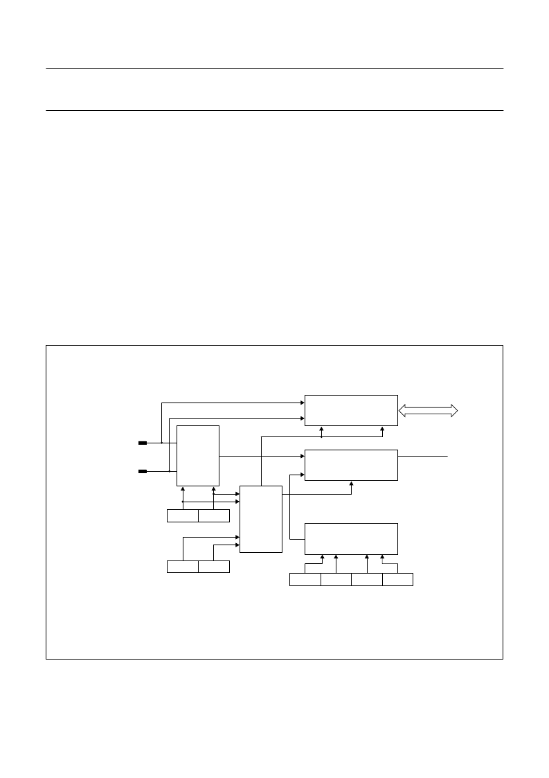
Fig.15 Block diagram of 2 channel ADC.
handbook, full pagewidth
4-BIT DAC
COMPARATOR
EN
DAC3
DAC2
DAC1
DAC0
ADCE1
ADCE2
ADCS1
ADCS0
MGD263
ADC enable selection
DAC value selection
ENABLE
SELECTOR
ADC
CHANNEL
SELECTOR
DP12/ADC2
DP11/ADC1
Vref
DERIVATIVE PORT
SELECTOR
EN1
EN2
‘MOV A, D20’
instruction
to read COMP bit
COMP bit
Internal bus
Channel selection
+
相關PDF資料 |
PDF描述 |
|---|---|
| PCF1000 | Analog IC |
| PCF600 | Analog IC |
| PCF1174C | 4-digit static LCD car clock |
| PCF1174CT | 4-digit static LCD car clock |
| PCF1174CU | 4-digit static LCD car clock |
相關代理商/技術參數 |
參數描述 |
|---|---|
| PCEA02 | 制造商:ADAM-TECH 制造商全稱:Adam Technologies, Inc. 功能描述:.100&.156 RECEPTACLE WITH BOARD HOOKS |
| PCE-A-05 | 制造商:ADAM-TECH 制造商全稱:Adam Technologies, Inc. 功能描述:.100 RECEPTACLE WITH BOARD HOOKS |
| PCEA10 | 制造商:ADAM-TECH 制造商全稱:Adam Technologies, Inc. 功能描述:.100&.156 RECEPTACLE WITH BOARD HOOKS |
| PCEA20 | 制造商:ADAM-TECH 制造商全稱:Adam Technologies, Inc. 功能描述:.100&.156 RECEPTACLE WITH BOARD HOOKS |
| PCEB02 | 制造商:ADAM-TECH 制造商全稱:Adam Technologies, Inc. 功能描述:.100&.156 RECEPTACLE WITH BOARD HOOKS |
發布緊急采購,3分鐘左右您將得到回復。