- 您現在的位置:買賣IC網 > PDF目錄374595 > RLD03N06CLESM (FAIRCHILD SEMICONDUCTOR CORP) 0.3A, 60V, ESD Rated, Current Limited, Voltage Clamped Logic Level N-Channel Enhancement-Mode Power MOSFETs PDF資料下載
參數資料
| 型號: | RLD03N06CLESM |
| 廠商: | FAIRCHILD SEMICONDUCTOR CORP |
| 元件分類: | JFETs |
| 英文描述: | 0.3A, 60V, ESD Rated, Current Limited, Voltage Clamped Logic Level N-Channel Enhancement-Mode Power MOSFETs |
| 中文描述: | 60 V, 6 ohm, N-CHANNEL, Si, POWER, MOSFET, TO-252AA |
| 文件頁數: | 1/13頁 |
| 文件大小: | 188K |
| 代理商: | RLD03N06CLESM |
CAUTION: These devices are sensitive to electrostatic discharge. Users should follow proper ESD Handling Procedures.
Copyright
Harris Corporation 1996
1
S E M I C O N D U C T O R
RLD03N06CLE,
RLD03N06CLESM, RLP03N06CLE
0.3A, 60V, ESD Rated, Current Limited, Voltage Clamped
Logic Level N-Channel Enhancement-Mode Power MOSFETs
July 1996
Absolute Maximum Ratings
T
C
= +25
o
C
RLD03N06CLE,
RLD03N06CLESM,
RLP03N06CLE
60
60
+5.5
UNITS
V
V
V
Drain Source Voltage . . . . . . . . . . . . . . . . . . . . . . . . . . . . . . . . . . . . . . . . . . . . . . . . . . . . .V
DSS
Drain Gate Voltage. . . . . . . . . . . . . . . . . . . . . . . . . . . . . . . . . . . . . . . . . . . . . . . . . . . . . . V
DGR
Gate Source Voltage (Note). . . . . . . . . . . . . . . . . . . . . . . . . . . . . . . . . . . . . . . . . . . . . . . . V
GS
Reverse Voltage Gate Bias Not Allowed
Drain Current
RMS Continuous. . . . . . . . . . . . . . . . . . . . . . . . . . . . . . . . . . . . . . . . . . . . . . . . . . . . . . . . . I
D
Power Dissipation
T
C
= +25
o
C . . . . . . . . . . . . . . . . . . . . . . . . . . . . . . . . . . . . . . . . . . . . . . . . . . . . . . . . . . . . P
D
Derate above +25
o
C. . . . . . . . . . . . . . . . . . . . . . . . . . . . . . . . . . . . . . . . . . . . . . . . . . . . . .P
T
Electrostatic Discharge Rating MIL-STD-883, Category B(2) . . . . . . . . . . . . . . . . . . . . . . ESD
Operating and Storage Temperature . . . . . . . . . . . . . . . . . . . . . . . . . . . . . . . . . . . . . .T
STG
, T
J
Self Limited
30
0.2
2
W
W/
o
C
KV
o
C
-55 to +175
File Number
3948.3
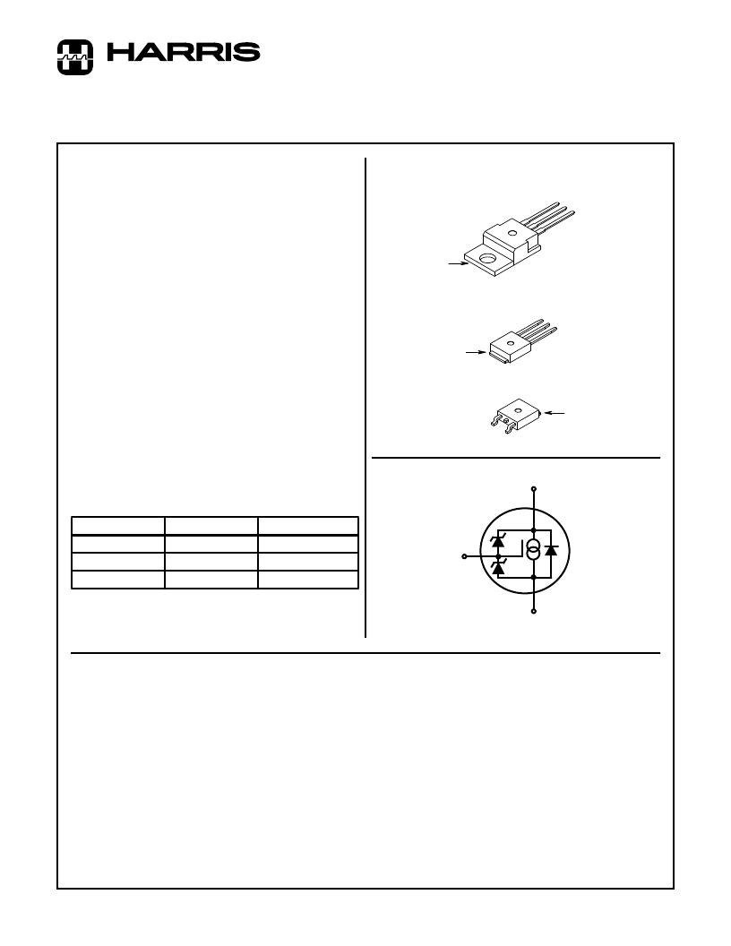
Packages
JEDEC TO-220AB
JEDEC TO-251AA
JEDEC TO-252AA
Symbol
DRAIN
(FLANGE)
SOURCE
DRAIN
GATE
SOURCE
DRAIN
GATE
DRAIN
(FLANGE)
SOURCE
GATE
DRAIN
(FLANGE)
G
S
D
Features
0.30A, 60V
r
DS(ON)
= 6.0
Built in Current Limit I
LIMIT
0.140 to 0.210A at 150
o
C
Built in Voltage Clamp
Temperature CompensatingPSPICE Model
2kV ESD Protected
Controlled Switching Limits EMI and RFI
Description
The RLD03N06CLE, RLD03N06CLESM and RLP03N06CLE
are intelligent monolithic power circuits which incorporate a lat-
eral bipolar transistor, resistors, zener diodes and a power MOS
transistor. The current limiting of these devices allow it to be used
safely in circuits where a shorted load condition may be encoun-
tered. The drain-source voltage clamping offers precision control
of the circuit voltage when switching inductive loads. The “Logic
Level” gate allows this device to be fully biased on with only 5.0V
from gate to source, thereby facilitating true on-off power control
directly from logic level (5V) integrated circuits.
The RLD03N06CLE, RLD03N06CLESM and RLP03N06CLE
incorporate ESD protection and are designed to withstand 2kV
(Human Body Model) of ESD.
Formerly developmental type TA49026.
PACKAGING AVAILABILITY
PART NUMBER
PACKAGE
BRAND
RLD03N06CLE
TO-251AA
03N06C
RLD03N06CLESM
TO-252AA
03N06C
RLP03N06CLE
TO-220AB
03N06CLE
NOTE: When ordering, use the entire part number. Add the suffix 9A
to obtain the TO-252AA variant in tape and reel, i.e.
RLD03N06CLESM9A.
相關PDF資料 |
PDF描述 |
|---|---|
| RLP1N06CLE | 1A, 55V, 0.750 Ohm,Voltage Clamping,Current Limited, N-Channel Power MOSFET(1A, 55V, 0.750 Ω,電壓箝位,電流限定,N溝道功率MOS場效應管) |
| RLP1N08LE | 1A, 80V, 0.750 Ohm, Current Limited, N-Channel Power MOSFET |
| RM100D2Z-40 | HIGH VOLTAGE MEDIUM POWER GENERAL USE INSULATED TYPE |
| RM100DZ-2H | HIGH VOLTAGE MEDIUM POWER GENERAL USE INSULATED TYPE |
| RM100CZ-24 | HIGH VOLTAGE MEDIUM POWER GENERAL USE INSULATED TYPE |
相關代理商/技術參數 |
參數描述 |
|---|---|
| RLD03N06CLESM9A | 制造商:Rochester Electronics LLC 功能描述:- Bulk |
| RLD06P075B | 制造商:LITTELFUSE 制造商全稱:Littelfuse 功能描述:This new radial leaded products are designed specifi cally for Universal Serial Bus (USB |
| RLD06P075BA | 功能描述:可復位保險絲 - RoHS:否 制造商:Bourns 電流額定值: 電阻:7.5 Ohms 最大直流電壓: 保持電流:0.1 A 安裝風格:SMD/SMT 端接類型:SMD/SMT 跳閘電流:0.6 A 引線間隔: 系列:MF-PSHT 工作溫度范圍:- 40 C to + 125 C |
| RLD06P075BF | 功能描述:可復位保險絲 6V .75A RoHS:否 制造商:Bourns 電流額定值: 電阻:7.5 Ohms 最大直流電壓: 保持電流:0.1 A 安裝風格:SMD/SMT 端接類型:SMD/SMT 跳閘電流:0.6 A 引線間隔: 系列:MF-PSHT 工作溫度范圍:- 40 C to + 125 C |
| RLD06P120B | 制造商:LITTELFUSE 制造商全稱:Littelfuse 功能描述:This new radial leaded products are designed specifi cally for Universal Serial Bus (USB |
發布緊急采購,3分鐘左右您將得到回復。