- 您現在的位置:買賣IC網 > Datasheet目錄46 > SC2463TSTRT (Semtech)IC REG QD BCK/LINEAR 28TSSOP Datasheet資料下載
參數資料
| 型號: | SC2463TSTRT |
| 廠商: | Semtech |
| 文件頁數: | 19/23頁 |
| 文件大小: | 459K |
| 描述: | IC REG QD BCK/LINEAR 28TSSOP |
| 標準包裝: | 1 |
| 拓撲: | 降壓(降壓)同步(2),線性(LDO)(2) |
| 功能: | 任何功能 |
| 輸出數: | 4 |
| 頻率 - 開關: | 600kHz |
| 電壓/電流 - 輸出 1: | 控制器 |
| 電壓/電流 - 輸出 2: | 控制器 |
| 電壓/電流 - 輸出 3: | 控制器 |
| 帶 LED 驅動器: | 無 |
| 帶監控器: | 無 |
| 帶序列發生器: | 是 |
| 電源電壓: | 4.5 V ~ 30 V |
| 工作溫度: | -40°C ~ 105°C |
| 安裝類型: | 表面貼裝 |
| 封裝/外殼: | 28-TSSOP(0.173",4.40mm 寬) |
| 供應商設備封裝: | 28-TSSOP |
| 包裝: | 標準包裝 |
| 產品目錄頁面: | 1358 (CN2011-ZH PDF) |
| 其它名稱: | SC2463TSDKR |
19
?2007 Semtech Corp.
www.semtech.com
SC2463
POWER MANAGEMENT
Applications Information (Cont.)
3. Select ?/SPAN>
Z1
and ?/SPAN>
Z2
such that they are placed near ?/SPAN>
O
to dampen peaking; the loop gain has 20dB rate
to go across the 0dB line for obtaining a wide band-
width.
4. Cancel ?/SPAN>
ESR
with compensation pole ?/SPAN>
P1
(?/SPAN>
P1
= ?/SPAN>
ESR
).
5. Place a high frequency compensation pole ?/SPAN>
P2
at the
half switching frequency to get the maximum attenu-
ation of the switching ripple and the high frequency
noise with the adequate phase lag at ?/SPAN>
C
.
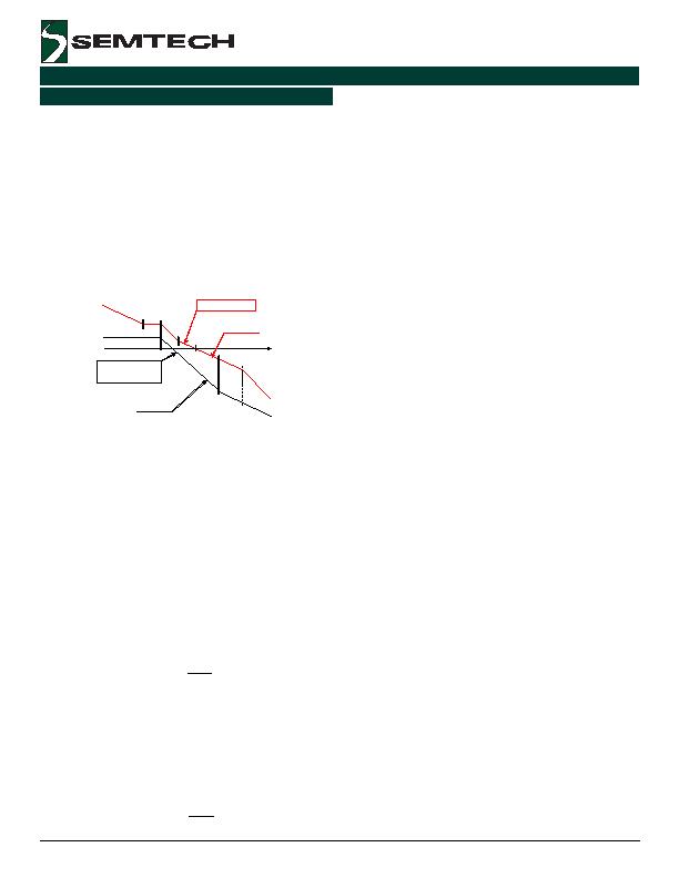
The compensated loop gain will be as given in Figure 8:
-20dB/dec
0dB
Gvd
T(s)
?/DIV>
z1
?/DIV>
z2
?/DIV>
o
?/DIV>
c
?/DIV>
p1
?/DIV>
ESR
?/DIV>
p2
Loop gain T(s)
Power stage
G
VD
(s)
-40dB/dec
-20dB/dec
0dB
Gvd
T(s)
?/DIV>
z1
?/DIV>
z2
?/DIV>
o
?/DIV>
c
?/DIV>
p1
?/DIV>
ESR
?/DIV>
p2
Loop gain T(s)
Power stage
G
VD
(s)
-40dB/dec
Figure 8. Asymptotic diagram of buck power stage and
its compensated loop gain
Dual Positive LDOs Controller
The SC2463 provides two positive adjustable linear regu-
lator controllers. The first positive linear regulator uses a
PNP transistor to regulate output voltage. This is set by
a voltage divider connected from the output to FB to
AGND. Referring to the front page Application Circuit,
select R10 in the 5K& to 20K& range. Calculate R9 with
the following equation:
?/DIV>
?/DIV>
?/DIV>
?/DIV>
?/DIV>
?/DIV>
=
1
5
.
0
V
R
R
OUT
10
9
The second positive linear regulator uses a NPN transis-
tor to regulate output voltage. This is set by a voltage
divider connected from the output to FB to AGND. Re-
ferring to the front page Application Circuit, select R18
in the 5K& to 20K& range. Calculate R14 with the
following equation:
?/DIV>
?/DIV>
主站蜘蛛池模板:
鹿邑县|
沙雅县|
武威市|
华阴市|
盐山县|
贵溪市|
长垣县|
松滋市|
中西区|
渑池县|
柘城县|
兴隆县|
房产|
云阳县|
杂多县|
玉门市|
翁源县|
运城市|
张家川|
都江堰市|
建水县|
奉贤区|
象州县|
瑞金市|
洪泽县|
奉节县|
武平县|
霍城县|
玛沁县|
日土县|
万年县|
准格尔旗|
闸北区|
灌阳县|
扎赉特旗|
潮州市|
德格县|
花垣县|
曲靖市|
安顺市|
应用必备|
?/DIV>
?/DIV>
?/DIV>
?/DIV>
=
1
5
.
0
V
R
R
OUT
18
14
The maximum voltage to drive an NPN transistor is AVCC
minus the voltage drop across the internal P-MOSFET
which is the product of On-Resistance and sourcing cur-
rent. The maximum driving voltage with 5mA sourcing
current is minimum AVCC (4.5V) minus 5mA times maxi-
mum On-Resistance 140&, i.e. 3.8V.
Layout Guidelines
Layout Guidelines
Layout Guidelines
Layout Guidelines
Layout Guidelines
In order to achieve optimal electrical, thermal and noise
performance for high frequency converters, attention
must be paid to the PCB layouts. The goal of layout opti-
mization is to place components properly and identify
the high di/dt loops to minimize them. The following guide-
lines should be used to ensure proper functions of the
converters:
1. A ground plane is recommended to minimize noises
and copper losses, and maximize heat dissipation.
2. Start the PCB layout by placing the power compo-
nents first. Arrange the power circuit to achieve a
clean power flow route. Put all the connections on
one side of the PCB with wide copper filled areas if
possible.
3. The PVCC and AVCC bypass capacitors should be
placed next to the PVCC, AVCC and PGND, AGND pins
respectively.
4. Separate the power ground from the signal ground.
In SC2463, the power ground PGND should be tied
to the source terminal of lower MOSFETs. The signal
ground AGND should be tied to the negative termi-
nal of the output capacitor.
5. The trace connecting the feedback resistors to the
output should be short, direct and far away from the
noise sources such as switching node and switching
components. Minimize the traces between DRXH/
DRXL and the gates of the MOSFETs to reduce their
impedance to drive the MOSFETs.
7. Minimize the loop including input capacitors, top/bot-
tom MOSFETs. This loop passes high di/dt current.
Make sure the trace width is wide enough to reduce
copper losses in this loop.
8. Maximize the trace width of the loop connecting the
inductor, bottom MOSFET and the output capacitors.
9. Connect the ground of the feedback divider and the
compensation components directly to the GND pin
of the SC2463 by using a separate ground trace.
Then connect this pin to the ground of the output
capacitor as close as possible.
相關PDF資料 |
PDF描述 |
|---|---|
| SC338AIMSTRT | IC REG CTRLR DUAL POS ADJ 10MSOP |
| SC402BMLTRT | IC REG DL BCK/LINEAR SYNC 32MLPQ |
| SC403MLTRT | IC REG DL BCK/LINEAR SYNC 32MLPQ |
| SC418ULTRT | IC REG DL BUCK/LINEAR 20MLPQ |
| SC424MLTRT | IC REG DL BUCK/LINEAR 28MLPQ |
相關代理商/技術參數 |
參數描述 |
|---|---|
| SC24-681-R | 功能描述:INDUCTOR SHIELD 680UH 40MA SMD RoHS:是 類別:電感器,線圈,扼流圈 >> 固定式 系列:SC24 標準包裝:500 系列:1331 電感:1.2µH 電流:247mA 電流 - 飽和:247mA 電流 - 溫升:- 類型:鐵芯體 容差:±10% 屏蔽:屏蔽 DC 電阻(DCR):最大 730 毫歐 Q因子@頻率:40 @ 7.9MHz 頻率 - 自諧振:130MHz 材料 - 芯體:鐵 封裝/外殼:0.312" L x 0.115" W x 0.135" H(7.94mm x 2.92mm x 3.43mm) 安裝類型:表面貼裝 包裝:帶卷 (TR) 工作溫度:-55°C ~ 105°C 頻率 - 測試:7.9MHz |
| SC246B | 制造商:Genteq 功能描述: 制造商:GENTEQ / GE 功能描述: |
| SC246D | 制造商:未知廠家 制造商全稱:未知廠家 功能描述:TRIAC|400V V(DRM)|10A I(T)RMS|TO-203AA |
| SC246M | 制造商:未知廠家 制造商全稱:未知廠家 功能描述:TRIAC|600V V(DRM)|10A I(T)RMS|TO-203AA |
| SC2475 | 制造商:SYSTEMSENSOR 制造商全稱:SYSTEMSENSOR 功能描述:Strobes and Horn Strobes |
發布緊急采購,3分鐘左右您將得到回復。