- 您現(xiàn)在的位置:買(mǎi)賣(mài)IC網(wǎng) > Datasheet目錄46 > SC402BMLTRT (Semtech)IC REG DL BCK/LINEAR SYNC 32MLPQ Datasheet資料下載
參數(shù)資料
| 型號(hào): | SC402BMLTRT |
| 廠商: | Semtech |
| 文件頁(yè)數(shù): | 21/32頁(yè) |
| 文件大小: | 1425K |
| 描述: | IC REG DL BCK/LINEAR SYNC 32MLPQ |
| 標(biāo)準(zhǔn)包裝: | 1 |
| 系列: | EcoSpeed®, SmartDrive™ |
| 拓?fù)洌?/td> | 降壓(降壓)同步(1),線性(LDO)(1) |
| 功能: | 任何功能 |
| 輸出數(shù): | 2 |
| 頻率 - 開(kāi)關(guān): | 1MHz |
| 電壓/電流 - 輸出 1: | 可調(diào)至 0.6V,10A |
| 電壓/電流 - 輸出 2: | 可調(diào)至 0.75V,200mA |
| 帶 LED 驅(qū)動(dòng)器: | 無(wú) |
| 帶監(jiān)控器: | 無(wú) |
| 帶序列發(fā)生器: | 是 |
| 電源電壓: | 3 V ~ 28 V |
| 工作溫度: | -40°C ~ 85°C |
| 安裝類(lèi)型: | 表面貼裝 |
| 封裝/外殼: | 32-VFQFN 裸露焊盤(pán) |
| 供應(yīng)商設(shè)備封裝: | 32-MLPQ(5x5) |
| 包裝: | 標(biāo)準(zhǔn)包裝 |
| 其它名稱(chēng): | SC402BMLDKR |
第1頁(yè)第2頁(yè)第3頁(yè)第4頁(yè)第5頁(yè)第6頁(yè)第7頁(yè)第8頁(yè)第9頁(yè)第10頁(yè)第11頁(yè)第12頁(yè)第13頁(yè)第14頁(yè)第15頁(yè)第16頁(yè)第17頁(yè)第18頁(yè)第19頁(yè)第20頁(yè)當(dāng)前第21頁(yè)第22頁(yè)第23頁(yè)第24頁(yè)第25頁(yè)第26頁(yè)第27頁(yè)第28頁(yè)第29頁(yè)第30頁(yè)第31頁(yè)第32頁(yè)
SC402B
21
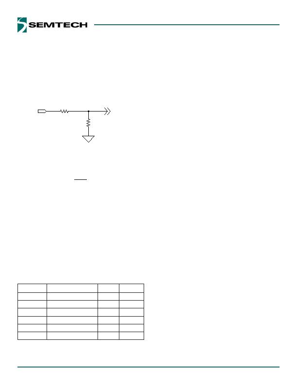
LDO Regulator
SC402B has an option to bias the switcher by using an
internal LDO from V
IN
. The LDO output is connected to
VDD internally. The output of the LDO is programmable
by using external resistors from the VDD pin to AGND (see
Figure 9). The feedback pin (FBL) for the LDO is regulated
to 750mV.
Figure 9 LDO Output Voltage Selection
The LDO output voltage is set by the following equation.
2
LDO
1
LDO
R
R
1
mV
750
VLDO
A minimum capacitance of 1糉 referenced to AGND is
normally required at the output of the LDO for stability.
Note that if the LDO voltage is set lower than 4.5V, the
minimum output capacitance for the LDO is 10uF.
LDO ENL Functions
The ENL input is used to enable/disable the internal LDO.
When ENL is a logic low, the LDO is off. When ENL is above
the V
IN
UVLO threshold, the LDO is enabled and the switcher
is also enabled if the EN/PSV and VDD are above their
threshold. The table below summarizes the function of ENL
and EN/PSV pins.
EN/PSV
ENL
LDO Switcher
Disabled Low, < 0.4V OFF OFF
Enabled Low, < 0.4V OFF ON
Disabled 1.0V < High < 2.6V ON OFF
Enabled 1.0V < High < 2.6V ON OFF
Disabled High, > 2.6V ON OFF
Enabled High, > 2.6V ON ON
The ENL pin also acts as the switcher under-voltage lockout
for the V
IN
supply. When SC402B is self-biased from the LDO
and runs from the V
IN
power source only, the V
IN
UVLO
feature can be used to prevent false UV faults for the PWM
output by programming with a resistor divider at the VIN,
ENL and AGND pins. When SC402B has an external bias
voltage at VDD and the ENL pin is used to program the V
IN
UVLO feature, the voltage at FBL needs to be higher than
750mV to force the LDO off.
Timing is important when driving ENL with logic and not
implementing V
IN
UVLO. The ENL pin must transition from
high to low within 2 switching cycles to avoid the PWM
output turning off. If ENL goes below the VIN UVLO
threshold and stays above 1V, then the switcher will turn
off but the LDO will remain on.
LDO Start-up
Before start-up, the LDO checks the status of the following
signals to ensure proper operation can be maintained.
ENL pin
V
IN
input voltage
When the ENL pin is high and V
IN
is above the UVLO point,
the LDO will begin start-up. During the initial phase, when
the V
DD
voltage (which is the LDO output voltage) is less
than 0.75V, the LDO initiates a current-limited start-up
(typically 65mA) to charge the output capacitors while
protecting from a short circuit event. When V
DD
is greater
than 0.75V but still less than 90% of its final value (as
sensed at the FBL pin), the LDO current limit is increased
to ~115mA. When V
DD
has reached 90% of the final value
(as sensed at the FBL pin), the LDO current limit is increased
to ~200mA and the LDO output is quickly driven to the
nominal value by the internal LDO regulator. It is recom-
mended that during LDO start-up to hold the PWM
switching off until the LDO has reached 90% of the final
value. This prevents overloading the current-limited LDO
output during the LDO start-up.
1.
2.
Applications Information (continued)
相關(guān)PDF資料 |
PDF描述 |
|---|---|
| SC403MLTRT | IC REG DL BCK/LINEAR SYNC 32MLPQ |
| SC418ULTRT | IC REG DL BUCK/LINEAR 20MLPQ |
| SC424MLTRT | IC REG DL BUCK/LINEAR 28MLPQ |
| SC4250LISTRT | IC HOT SWAP CTRLR 8-SOIC |
| SC427MLTRT | IC REG DL BUCK/LINEAR 32MLPQ |
相關(guān)代理商/技術(shù)參數(shù) |
參數(shù)描述 |
|---|---|
| SC402S | 功能描述:數(shù)據(jù)轉(zhuǎn)換模塊 SC400 4W SERIAL OEM RoHS:否 制造商:Lyrtech 產(chǎn)品:ADC and DAC FMC Modules 轉(zhuǎn)換速率:250 MSPS, 1 GSPS 信噪比: ADC 輸入端數(shù)量:2 DAC 輸出端數(shù)量:2 分辨率:14 bit, 16 bit 接口類(lèi)型:SPI 工作電源電壓:3.3 V, 12 V 工作電源電流: 最大工作溫度: 尺寸:84 mm x 69 mm x 10 mm |
| SC403 | 制造商:SEMTECH 制造商全稱(chēng):Semtech Corporation 功能描述:6A EcoSpeedTM Integrated FET Regulator with Programmable LDO |
| SC403B | 制造商:SEMTECH 制造商全稱(chēng):Semtech Corporation 功能描述:6A EcoSpeed?? Integrated FET Regulator with Programmable LDO |
| SC403BEVB | 制造商:SEMTECH 功能描述:Evaluation Board for 10 A EcoSpeed?Integrated FET Regulator w/ Programmable LDO |
| SC403BMLTRT | 制造商:Semtech Corporation 功能描述:Integrated FET Regulator with Programmable LDO 32-Pin MLPQ T/R 制造商:Semtech Corporation 功能描述:6A EcoSpeed Integrated FET Regulator with Programmable LDO. PKG: MLPQ-32 制造商:Semtech 功能描述:Integrated FET Regulator with Programmable LDO 32-Pin MLPQ T/R 制造商:SEMTECH 功能描述:6A EcoSpeed step down regultor |
發(fā)布緊急采購(gòu),3分鐘左右您將得到回復(fù)。