- 您現(xiàn)在的位置:買賣IC網(wǎng) > PDF目錄98239 > TLC4545IDRG4 (TEXAS INSTRUMENTS INC) 1-CH 16-BIT SUCCESSIVE APPROXIMATION ADC, SERIAL ACCESS, PDSO8 PDF資料下載
參數(shù)資料
| 型號: | TLC4545IDRG4 |
| 廠商: | TEXAS INSTRUMENTS INC |
| 元件分類: | ADC |
| 英文描述: | 1-CH 16-BIT SUCCESSIVE APPROXIMATION ADC, SERIAL ACCESS, PDSO8 |
| 封裝: | GREEN, PLASTIC, MS-012AA, SOIC-8 |
| 文件頁數(shù): | 6/26頁 |
| 文件大小: | 652K |
| 代理商: | TLC4545IDRG4 |
TLC4541, TLC4545
SLAS293 DECEMBER 2001
14
www.ti.com
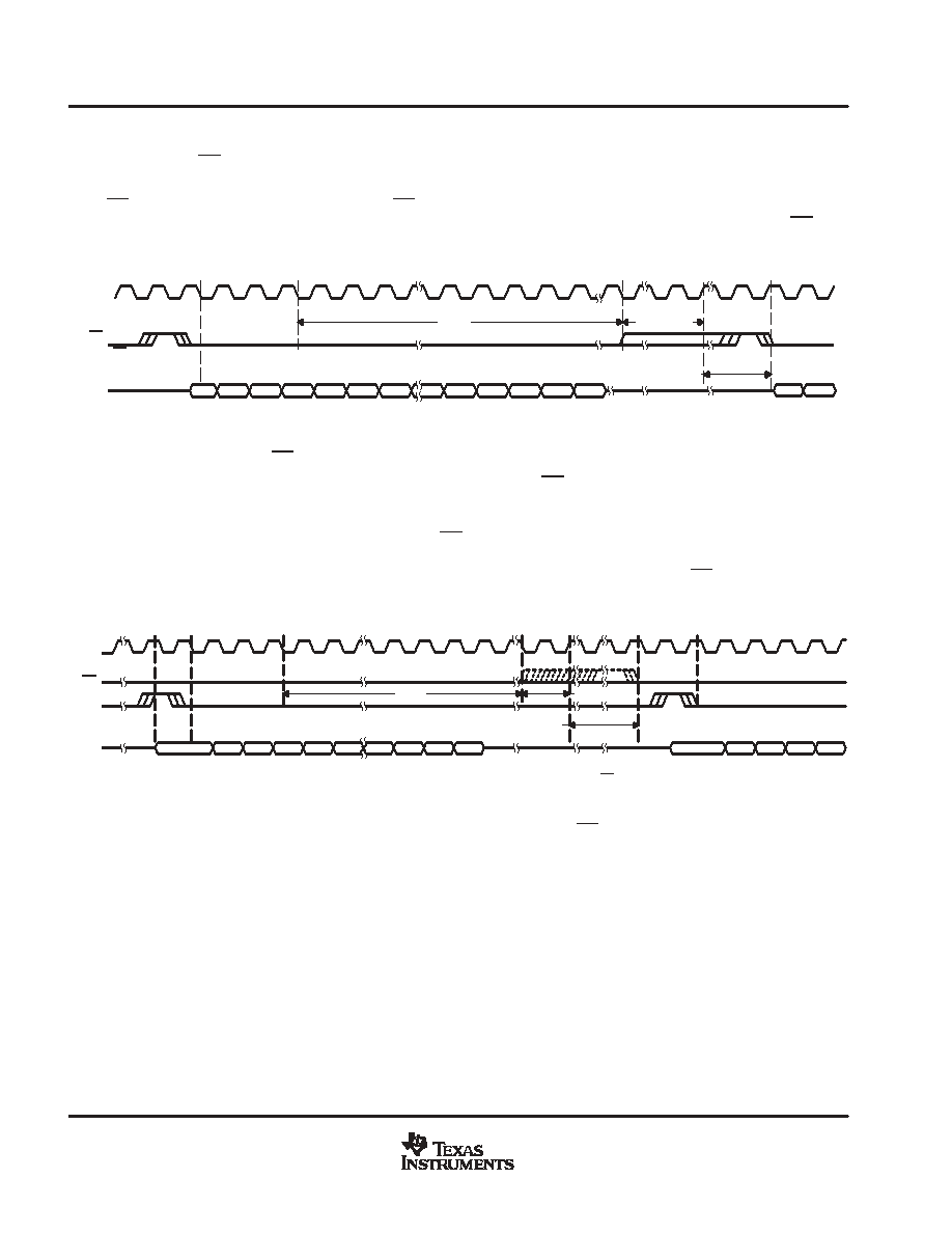
PRINCIPLES OF OPERATION
control via pin 1 (CS, DSP interface)
All devices are compatible with this mode of operation. The FS signal from a DSP is connected directly to the
CS input of the ADC. A falling edge on the CS input while SCLK is high or low initiates the cycle. (For TLC4541
in this configuration, the FS input is tied to VDD.) Enough time should be allowed before the next rising CS edge
so that the conversion cycle is not terminated prematurely.
1
2
3
5
4
6
7
13
14
15
16
1
12
ts
tconv
t(PWRDWN)
SDO Data is the Result of the Previous Sample
For TLC45xx, the LSB is Presented on the Rising SCLK 16th Edge
MSB
MSB1
MSB2 MSB3 MSB4 MSB5 MSB6
LSB4
LSB3
LSB2
LSB1
LSB
SCLK
CS
SDO
MSB
MSB1
The CS Input Signal is
Generated by the FS Output
From a TMS320 DSP
24
Figure 16. DSP Cycle Timing Using the CS Input (FS = 1 for TLC4541 Only)
control via pin 1 and pin 7 (CS and FS or FS only, DSP interface)
Only TLC4541 is compatible with this mode of operation. The CS input to the ADC can be controlled via a
general-purpose I/O pin from the DSP or tied to ground. The FS signal from the DSP is connected directly to
the FS input of the ADC. A rising FS edge releases the MSB to the SDO output. The falling edge on the FS input
while SCLK is high or low initiates the cycle. The CS input should remain low for the entire sampling time plus
4 SCLK decoding time after falling FS (24 falling SCLK edges) and can then be released at any time during the
remainder of the conversion cycle. The optimum DSP interface is achieved when tying CS to ground and using
only the FS input to control the ADC.
tconv
t(PWRDWN)
SDO Data is the Result of the Previous Sample
For TLC45xx, the LSB is Presented on the Rising SCLK 16th Edge
1
2
3
5
4
6
14
15
16
1
2
34
ts
MSB
MSB1 MSB2 MSB3 MSB4 MSB5 LSB3
LSB2 LSB1
LSB
MSB
MSB1 MSB2 MSB3
The MSB is Presented on the SDO Output After
a Rising Edge on the FS Input.
17
24
The Device Will go into the Power Down State After the Conversion is
Complete. A Falling CS Edge or Rising FS Edge, Whichever Occurs First,
Removes the Device From Power Down.
SCLK
CS
SDO
FS
Figure 17. DSP Cycle Timing Using FS Only (or Using Both CS and FS for the TLC4541)
相關PDF資料 |
PDF描述 |
|---|---|
| TLC4541IDR | 1-CH 16-BIT SUCCESSIVE APPROXIMATION ADC, SERIAL ACCESS, PDSO8 |
| TLC4545IDGK | 1-CH 16-BIT SUCCESSIVE APPROXIMATION ADC, SERIAL ACCESS, PDSO8 |
| TLC4545IDGKRG4 | 1-CH 16-BIT SUCCESSIVE APPROXIMATION ADC, SERIAL ACCESS, PDSO8 |
| TLC4541IDRG4 | 1-CH 16-BIT SUCCESSIVE APPROXIMATION ADC, SERIAL ACCESS, PDSO8 |
| TLC540INSG4 | 11-CH 8-BIT SUCCESSIVE APPROXIMATION ADC, SERIAL ACCESS, PDSO20 |
相關代理商/技術參數(shù) |
參數(shù)描述 |
|---|---|
| TLC-4C-0375 | 制造商:KATO/COILTHREAD 功能描述: |
| TLC-4C-0375W | 制造商:KATO/COILTHREAD 功能描述: |
| TLC-4C-0500 | 制造商:KATO/COILTHREAD 功能描述: |
| TL-C5-140-30 | 制造商:Newport Electronics Inc 功能描述:5-DOT ROUND LABELS |
| TLC530FTU | 功能描述:基準電壓& 基準電流 NPN 330V 7A RoHS:否 制造商:STMicroelectronics 產品:Voltage References 拓撲結構:Shunt References 參考類型:Programmable 輸出電壓:1.24 V to 18 V 初始準確度:0.25 % 平均溫度系數(shù)(典型值):100 PPM / C 串聯(lián) VREF - 輸入電壓(最大值): 串聯(lián) VREF - 輸入電壓(最小值): 分流電流(最大值):60 mA 最大工作溫度:+ 125 C 封裝 / 箱體:SOT-23-3L 封裝:Reel |
發(fā)布緊急采購,3分鐘左右您將得到回復。