- 您現在的位置:買賣IC網 > PDF目錄98252 > TLV2556MPWREPG4 (TEXAS INSTRUMENTS INC) 11-CH 12-BIT SUCCESSIVE APPROXIMATION ADC, SERIAL ACCESS, PDSO20 PDF資料下載
參數資料
| 型號: | TLV2556MPWREPG4 |
| 廠商: | TEXAS INSTRUMENTS INC |
| 元件分類: | ADC |
| 英文描述: | 11-CH 12-BIT SUCCESSIVE APPROXIMATION ADC, SERIAL ACCESS, PDSO20 |
| 封裝: | GREEN, PLASTIC, TSSOP-20 |
| 文件頁數: | 23/37頁 |
| 文件大小: | 705K |
| 代理商: | TLV2556MPWREPG4 |
第1頁第2頁第3頁第4頁第5頁第6頁第7頁第8頁第9頁第10頁第11頁第12頁第13頁第14頁第15頁第16頁第17頁第18頁第19頁第20頁第21頁第22頁當前第23頁第24頁第25頁第26頁第27頁第28頁第29頁第30頁第31頁第32頁第33頁第34頁第35頁第36頁第37頁
www.ti.com ................................................................................................................................................... SLAS598A – NOVEMBER 2008 – REVISED JULY 2009
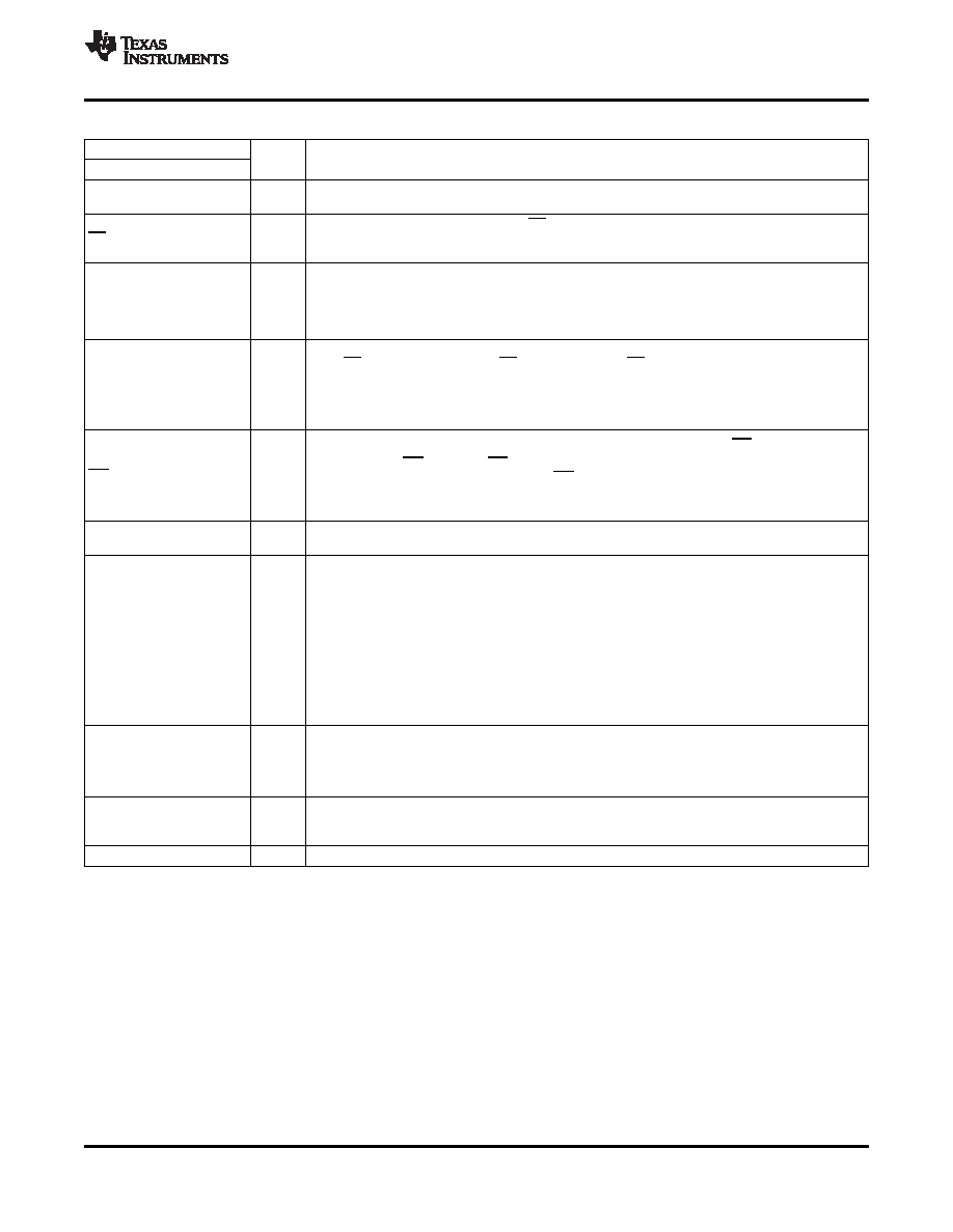
TERMINAL FUNCTIONS
TERMINAL
I/O
DESCRIPTION
NAME
NO.
1–9,
AIN0–AIN10
I
Analog input. These 11 analog-signal inputs are internally multiplexed.
11, 12
Chip select. A high-to-low transition on CS resets the internal counters and controls and enables
CS
15
I
DATA OUT, DATA IN, and I/O CLOCK. A low-to-high transition disables DATA IN and I/O CLOCK
within a setup time.
Serial data input. The 4-bit serial data can be used as address selects the desired analog input
channel or test voltage to be converted next, or a command to activate other features. The input
DATA IN
17
I
data is presented with the MSB (D7) first and is shifted in on the first four rising edges of the I/O
CLOCK. After the four address/command bits are read into the command register CMR, I/O
CLOCK clocks the remaining four bits of configuration in.
The 3-state serial output for the A/D conversion result. DATA OUT is in the high-impedance state
when CS is high and active when CS is low. With a valid CS, DATA OUT is removed from the
high-impedance state and is driven to the logic level corresponding to the MSB(most significant
DATA OUT
16
O
bit)/LSB(least significant bit) value of the previous conversion result. The next falling edge of I/O
CLOCK drives DATA OUT to the logic level corresponding to the next MSB/LSB, and the remaining
bits are shifted out in order.
Status output, used to indicate the end of conversion (EOC) or an interrupt (INT) to host processor.
Programmed as INT (interrupt): INT goes from a high to a low logic level after the conversion is
INT/EOC
19
O
complete and the data is ready for transfer. INT is cleared by a rising I/O CLOCK transition.
Programmed as EOC: EOC goes from a high to a low logic level after the falling edge of the last I/O
CLOCK and remains low until the conversion is complete and the data is ready for transfer.
Ground. GND is the ground return terminal for the internal circuitry. Unless otherwise noted, all
GND
10
voltage measurements are with respect to GND.
Input /output clock. I/O CLOCK receives the serial input and performs the following four functions:
1.
It clocks the eight input data bits into the input data register on the first eight rising edges of
I/O CLOCK with the multiplexer address available after the fourth rising edge.
2.
On the fourth falling edge of I/O CLOCK, the analog input voltage on the selected multiplexer
input begins charging the capacitor array and continues to do so until the last falling edge of
I/O CLOCK
18
I
I/O CLOCK.
3.
The remaining 11 bits of the previous conversion data are shifted out on DATA OUT. Data
changes on the falling edge of I/O CLOCK.
4.
Control of the conversion is transferred to the internal state controller on the falling edge of the
last I/O CLOCK.
Positive reference voltage The upper reference voltage value (nominally VCC) is applied to REF+.
The maximum analog input voltage range is determined by the difference between the voltage
REF+
14
I/O
applied to terminals REF+ and REF–.
When the internal reference is used it is capable of driving a 10-k
, 10-pF load.
Negative reference voltage. The lower reference voltage value (nominally ground) is applied to
REF–
13
I/O
REF–. This pin is connected to analog ground (GND of the ADC) when the internal reference is
used.
VCC
20
Positive supply voltage
Copyright 2008–2009, Texas Instruments Incorporated
3
Product Folder Link(s): TLV2556-EP
相關PDF資料 |
PDF描述 |
|---|---|
| TLV320ADC3001IYZHT | 2-CH 16-BIT PROPRIETARY METHOD ADC, SERIAL ACCESS, PBGA16 |
| TLV320ADC3001IYZHR | 2-CH 16-BIT PROPRIETARY METHOD ADC, SERIAL ACCESS, PBGA16 |
| TLV320ADC3101IRGER320 | SPECIALTY CONSUMER CIRCUIT, PQCC24 |
| TLV320ADC3101IRGET320 | SPECIALTY CONSUMER CIRCUIT, PQCC24 |
| TLV320ADC3101IRGER | SPECIALTY CONSUMER CIRCUIT, PQCC24 |
相關代理商/技術參數 |
參數描述 |
|---|---|
| TLV2620ID | 制造商:Rochester Electronics LLC 功能描述:- Bulk |
| TLV2620IDBVR | 功能描述:運算放大器 - 運放 800 uA/ch 11MHz RRO Lo-Vltg 1-Ch RoHS:否 制造商:STMicroelectronics 通道數量:4 共模抑制比(最小值):63 dB 輸入補償電壓:1 mV 輸入偏流(最大值):10 pA 工作電源電壓:2.7 V to 5.5 V 安裝風格:SMD/SMT 封裝 / 箱體:QFN-16 轉換速度:0.89 V/us 關閉:No 輸出電流:55 mA 最大工作溫度:+ 125 C 封裝:Reel |
| TLV2620IDBVRG4 | 功能描述:運算放大器 - 運放 800 uA/ch 11MHz RRO Lo-Vltg 1-Ch RoHS:否 制造商:STMicroelectronics 通道數量:4 共模抑制比(最小值):63 dB 輸入補償電壓:1 mV 輸入偏流(最大值):10 pA 工作電源電壓:2.7 V to 5.5 V 安裝風格:SMD/SMT 封裝 / 箱體:QFN-16 轉換速度:0.89 V/us 關閉:No 輸出電流:55 mA 最大工作溫度:+ 125 C 封裝:Reel |
| TLV2620IDBVT | 功能描述:運算放大器 - 運放 800 uA/ch 11MHz RRO Lo-Vltg 1-Ch RoHS:否 制造商:STMicroelectronics 通道數量:4 共模抑制比(最小值):63 dB 輸入補償電壓:1 mV 輸入偏流(最大值):10 pA 工作電源電壓:2.7 V to 5.5 V 安裝風格:SMD/SMT 封裝 / 箱體:QFN-16 轉換速度:0.89 V/us 關閉:No 輸出電流:55 mA 最大工作溫度:+ 125 C 封裝:Reel |
| TLV2620IDBVTG4 | 功能描述:運算放大器 - 運放 800 uA/ch 11MHz RRO Lo-Vltg 1-Ch RoHS:否 制造商:STMicroelectronics 通道數量:4 共模抑制比(最小值):63 dB 輸入補償電壓:1 mV 輸入偏流(最大值):10 pA 工作電源電壓:2.7 V to 5.5 V 安裝風格:SMD/SMT 封裝 / 箱體:QFN-16 轉換速度:0.89 V/us 關閉:No 輸出電流:55 mA 最大工作溫度:+ 125 C 封裝:Reel |
發布緊急采購,3分鐘左右您將得到回復。