- 您現(xiàn)在的位置:買賣IC網(wǎng) > PDF目錄98254 > TLV320AIC33IRGZTG4 (TEXAS INSTRUMENTS INC) SPECIALTY CONSUMER CIRCUIT, PQCC48 PDF資料下載
參數(shù)資料
| 型號: | TLV320AIC33IRGZTG4 |
| 廠商: | TEXAS INSTRUMENTS INC |
| 元件分類: | 消費家電 |
| 英文描述: | SPECIALTY CONSUMER CIRCUIT, PQCC48 |
| 封裝: | 7 X 7 MM, GREEN, PLASTIC, VQFN-48 |
| 文件頁數(shù): | 17/93頁 |
| 文件大小: | 1427K |
| 代理商: | TLV320AIC33IRGZTG4 |
第1頁第2頁第3頁第4頁第5頁第6頁第7頁第8頁第9頁第10頁第11頁第12頁第13頁第14頁第15頁第16頁當前第17頁第18頁第19頁第20頁第21頁第22頁第23頁第24頁第25頁第26頁第27頁第28頁第29頁第30頁第31頁第32頁第33頁第34頁第35頁第36頁第37頁第38頁第39頁第40頁第41頁第42頁第43頁第44頁第45頁第46頁第47頁第48頁第49頁第50頁第51頁第52頁第53頁第54頁第55頁第56頁第57頁第58頁第59頁第60頁第61頁第62頁第63頁第64頁第65頁第66頁第67頁第68頁第69頁第70頁第71頁第72頁第73頁第74頁第75頁第76頁第77頁第78頁第79頁第80頁第81頁第82頁第83頁第84頁第85頁第86頁第87頁第88頁第89頁第90頁第91頁第92頁第93頁
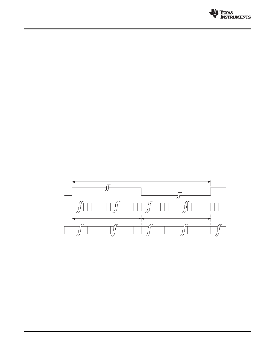
RIGHT JUSTIFIED MODE
BCLK
WCLK
SDIN/
SDOUT
n2
1
0
1
0
1/fs
LSB
MSB
LeftChannel
RightChannel
n3
2
n1
n2 n3
n1
LEFT JUSTIFIED MODE
SLAS480B – JANUARY 2006 – REVISED DECEMBER 2008 ........................................................................................................................................... www.ti.com
The word clock (WCLK or GPIO1) is used to define the beginning of a frame, and may be programmed as either
a pulse or a square-wave signal. The frequency of this clock corresponds to the maximum of the selected ADC
and DAC sampling frequencies.
The bit clock (BCLK or GPIO2) is used to clock in and out the digital audio data across the serial bus. When in
Master mode, this signal can be programmed in two further modes: continuous transfer mode, and 256-clock
mode. In continuous transfer mode, only the minimal number of bit clocks needed to transfer the audio data are
generated, so in general the number of bit clocks per frame will be two times the data width. For example, if data
width is chosen as 16-bits, then 32 bit clocks will be generated per frame. If the bit clock signal in master mode
will be used by a PLL in another device, it is recommended that the 16-bit or 32-bit data width selections be
used. These cases result in a low jitter bit clock signal being generated, having frequencies of 32×Fs or 64×Fs.
In the cases of 20-bit and 24-bt data width in master mode, the bit clocks generated in each frame will not all be
of equal period, due to the device not having a clean 40×Fs or 48×Fs clock signal readily available. The average
frequency of the bit clock signal is still accurate in these cases (being 40×Fs or 48×Fs), but the resulting clock
signal has higher jitter than in the 16-bit and 32-bit cases.
In 256-clock mode, a constant 256 bit clocks per frame are generated, independent of the data width chosen.
The TLV320AIC33 further includes programmability to tri-state the DOUT line during all bit clocks when valid
data is not being sent. By combining this capability with the ability to program at what bit clock in a frame the
audio data will begin, time-division multiplexing (TDM) can be accomplished, resulting in multiple codecs able to
use a single audio serial data bus.
When the audio serial data bus is powered down while configured in master mode, the pins associated with the
interface will be put into a tri-state output condition.
In right-justified mode, the LSB of the left channel is valid on the rising edge of the bit clock preceding the falling
edge of word clock. Similarly, the LSB of the right channel is valid on the rising edge of the bit clock preceding
the rising edge of the word clock.
Figure 22. Right Justified Serial Bus Mode Operation
In left-justified mode, the MSB of the right channel is valid on the rising edge of the bit clock following the falling
edge of the word clock. Similarly the MSB of the left channel is valid on the rising edge of the bit clock following
the rising edge of the word clock.
24
Copyright 2006–2008, Texas Instruments Incorporated
Product Folder Link(s): TLV320AIC33
相關(guān)PDF資料 |
PDF描述 |
|---|---|
| TLV320AIC33IRGZ | SPECIALTY CONSUMER CIRCUIT, PQCC48 |
| TLV320AIC36IZQER | SPECIALTY CONSUMER CIRCUIT, PBGA80 |
| TLV320AIC36IZQE | SPECIALTY CONSUMER CIRCUIT, PBGA80 |
| TLV320DAC23IPW | SERIAL INPUT LOADING, 32-BIT DAC, PDSO28 |
| TLV320DAC23IGQER | SERIAL INPUT LOADING, 32-BIT DAC, PBGA80 |
相關(guān)代理商/技術(shù)參數(shù) |
參數(shù)描述 |
|---|---|
| TLV320AIC33IZQE | 功能描述:接口—CODEC Lo-Pwr Stereo Codec w/6 Inp 7 Otp RoHS:否 制造商:Texas Instruments 類型: 分辨率: 轉(zhuǎn)換速率:48 kSPs 接口類型:I2C ADC 數(shù)量:2 DAC 數(shù)量:4 工作電源電壓:1.8 V, 2.1 V, 2.3 V to 5.5 V 最大工作溫度:+ 85 C 安裝風格:SMD/SMT 封裝 / 箱體:DSBGA-81 封裝:Reel |
| TLV320AIC33IZQE | 制造商:Texas Instruments 功能描述:AUDIO CODEC IC ((NW)) |
| TLV320AIC33IZQER | 功能描述:接口—CODEC Lo-Pwr Stereo Codec w/6 Inp 7 Otp RoHS:否 制造商:Texas Instruments 類型: 分辨率: 轉(zhuǎn)換速率:48 kSPs 接口類型:I2C ADC 數(shù)量:2 DAC 數(shù)量:4 工作電源電壓:1.8 V, 2.1 V, 2.3 V to 5.5 V 最大工作溫度:+ 85 C 安裝風格:SMD/SMT 封裝 / 箱體:DSBGA-81 封裝:Reel |
| TLV320AIC33NIZQE | 制造商:Texas Instruments 功能描述: |
| TLV320AIC33NIZQER | 制造商:Texas Instruments 功能描述: |
發(fā)布緊急采購,3分鐘左右您將得到回復。