- 您現在的位置:買賣IC網 > PDF目錄98258 > TLV5618AMDREPG4 (TEXAS INSTRUMENTS INC) SERIAL INPUT LOADING, 3 us SETTLING TIME, 12-BIT DAC, PDSO8 PDF資料下載
參數資料
| 型號: | TLV5618AMDREPG4 |
| 廠商: | TEXAS INSTRUMENTS INC |
| 元件分類: | DAC |
| 英文描述: | SERIAL INPUT LOADING, 3 us SETTLING TIME, 12-BIT DAC, PDSO8 |
| 封裝: | GREEN, SOIC-8 |
| 文件頁數: | 11/17頁 |
| 文件大小: | 389K |
| 代理商: | TLV5618AMDREPG4 |
TLV5618AEP
2.7V TO 5.5V LOW POWER DUAL 12BIT
DIGITALTOANALOG CONVERTER WITH POWER DOWN
SGLS214 OCTOBER 2003
3
POST OFFICE BOX 655303
DALLAS, TEXAS 75265
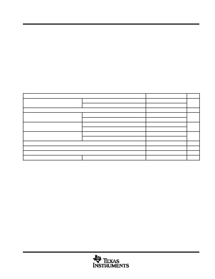
absolute maximum ratings over operating free-air temperature range (unless otherwise noted)
Supply voltage (VDD to AGND)
7 V
. . . . . . . . . . . . . . . . . . . . . . . . . . . . . . . . . . . . . . . . . . . . . . . . . . . . . . . . . . . . . . .
Reference input voltage range
0.3 V to VDD + 0.3 V
. . . . . . . . . . . . . . . . . . . . . . . . . . . . . . . . . . . . . . . . . . . . . . .
Digital input voltage range
0.3 V to VDD + 0.3 V
. . . . . . . . . . . . . . . . . . . . . . . . . . . . . . . . . . . . . . . . . . . . . . . . . .
Operating free-air temperature range, TA: TLV5618AM
55
°C to 125°C
. . . . . . . . . . . . . . . . . . . . . . . . . . . . . .
Storage temperature range, Tstg
65
°C to 150°C
. . . . . . . . . . . . . . . . . . . . . . . . . . . . . . . . . . . . . . . . . . . . . . . . . .
Lead temperature 1,6 mm (1/16 inch) from case for 10 seconds
260
°C
. . . . . . . . . . . . . . . . . . . . . . . . . . . . . . .
Package thermal impedance, R
θJA: D package
131
°C/W
. . . . . . . . . . . . . . . . . . . . . . . . . . . . . . . . . . . . . . . . . . . .
Stresses beyond those listed under “absolute maximum ratings” may cause permanent damage to the device. These are stress ratings only, and
functional operation of the device at these or any other conditions beyond those indicated under “recommended operating conditions” is not
implied. Exposure to absolute-maximum-rated conditions for extended periods may affect device reliability.
Long term hightemperature storage and/or extended use at maximum recommended operating conditions may result in a reduction of overall
device life. See http://www.ti.com/ep_quality for additional information on enhanced plastic packaging.
recommended operating conditions
MIN
NOM
MAX
UNIT
Supply voltage, VDD
VDD = 5 V
4.5
5
5.5
V
Supply voltage, VDD
VDD = 3 V
2.7
3
3.3
V
Power on reset
0.55
2
V
High-level digital input voltage, VIH
VDD = 2.7 V
2
V
High-level digital input voltage, VIH
VDD = 5.5 V
2.4
V
Low-level digital input voltage, VIL
VDD = 2.7 V
0.6
V
Low-level digital input voltage, VIL
VDD = 5.5 V
1
V
Reference voltage, Vref to REF terminal
VDD = 5 V (see Note 1)
AGND
2.048
VDD 1.5
V
Reference voltage, Vref to REF terminal
VDD = 3 V (see Note 1)
AGND
1.024
VDD 1.5
V
Load resistance, RL
2
k
Load capacitance, CL
100
pF
Clock frequency, f(CLK)
20
MHz
Operating free-air temperature, TA
TLV5618AM
55
125
°C
NOTE 1: Due to the x2 output buffer, a reference input voltage
≥ (VDD0.4 V)/2 causes clipping of the transfer function.
相關PDF資料 |
PDF描述 |
|---|---|
| TLV5618AMDREP | SERIAL INPUT LOADING, 3 us SETTLING TIME, 12-BIT DAC, PDSO8 |
| TLV5619CDW | PARALLEL, WORD INPUT LOADING, 1 us SETTLING TIME, 12-BIT DAC, PDSO20 |
| TLV5619IPW | PARALLEL, WORD INPUT LOADING, 1 us SETTLING TIME, 12-BIT DAC, PDSO20 |
| TLV5619CPWR | PARALLEL, WORD INPUT LOADING, 1 us SETTLING TIME, 12-BIT DAC, PDSO20 |
| TLV5619QDWG4 | PARALLEL, WORD INPUT LOADING, 1 us SETTLING TIME, 12-BIT DAC, PDSO20 |
相關代理商/技術參數 |
參數描述 |
|---|---|
| TLV5618AMFK | 制造商:TI 制造商全稱:Texas Instruments 功能描述:2.7-V TO 5.5-V LOW-POWER DUAL 12-BIT DIGITAL-TO-ANALOG CONVERTER WITH POWER DOWN |
| TLV5618AMFKB | 制造商:Texas Instruments 功能描述:12-BIT, 2.5 US DUAL DAC, SERIAL INPUT |
| TLV5618AMJG | 制造商:Texas Instruments 功能描述:DAC 2-CH Resistor-String 12-bit 8-Pin CDIP Tube |
| TLV5618AMJGB | 制造商:Texas Instruments 功能描述:DAC 2-CH Resistor-String 12-bit 8-Pin CDIP Tube |
| TLV5618AQD | 功能描述:數模轉換器- DAC Dual 12bit DAC RoHS:否 制造商:Texas Instruments 轉換器數量:1 DAC 輸出端數量:1 轉換速率:2 MSPs 分辨率:16 bit 接口類型:QSPI, SPI, Serial (3-Wire, Microwire) 穩定時間:1 us 最大工作溫度:+ 85 C 安裝風格:SMD/SMT 封裝 / 箱體:SOIC-14 封裝:Tube |
發布緊急采購,3分鐘左右您將得到回復。