- 您現在的位置:買賣IC網 > PDF目錄98300 > TS8388BCFS (E2V TECHNOLOGIES PLC) 1-CH 8-BIT PROPRIETARY METHOD ADC, PARALLEL ACCESS, CQFP68 PDF資料下載
參數資料
| 型號: | TS8388BCFS |
| 廠商: | E2V TECHNOLOGIES PLC |
| 元件分類: | ADC |
| 英文描述: | 1-CH 8-BIT PROPRIETARY METHOD ADC, PARALLEL ACCESS, CQFP68 |
| 封裝: | CERAMIC, QFP-68 |
| 文件頁數: | 26/62頁 |
| 文件大小: | 1267K |
| 代理商: | TS8388BCFS |
第1頁第2頁第3頁第4頁第5頁第6頁第7頁第8頁第9頁第10頁第11頁第12頁第13頁第14頁第15頁第16頁第17頁第18頁第19頁第20頁第21頁第22頁第23頁第24頁第25頁當前第26頁第27頁第28頁第29頁第30頁第31頁第32頁第33頁第34頁第35頁第36頁第37頁第38頁第39頁第40頁第41頁第42頁第43頁第44頁第45頁第46頁第47頁第48頁第49頁第50頁第51頁第52頁第53頁第54頁第55頁第56頁第57頁第58頁第59頁第60頁第61頁第62頁
32
0860E–BDC–05/07
TS8388B
e2v semiconductors SAS 2007
No performance degradation (that is: due to timing jitter) is observed in this particular single-ended con-
figuration up to 1.2 Gsps Nyquist conditions (F
IN = 600 MHz).
This is true so long as the inverted phase clock input pin is 50
terminated very closely to one of the
neighboring shield ground pins, which constitutes the local Ground reference for the inphase clock input.
Thus the TS8388B differential clock input buffer will fully reject the local ground noise (and any capaci-
tively and inductively coupled noise) as common mode effects. Moreover, a very low phase noise
sinewave generator must be used for enhanced jitter performance.
The typical inphase clock input amplitude is 1V peak to peak, centered on 0V (ground) common mode.
This corresponds to a typical clock input power level of 4 dBm into the 50
termination resistor. Do not
exceed 10 dBm to avoid saturation of the preamplifier input transistors.
The inverted phase clock input is grounded through the 50
termination resistor.
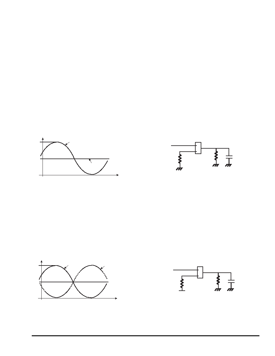
Figure 8-3.
Single-ended Clock Input (Ground common mode):
VCLK Common Mode = 0V; VCLKB = 0V; 4 dBm Typical Clock Input Power Level (into 50
termination
resistor)
Note:
Do not exceed 10 dBm into the 50
termination resistor for single clock input power level.
8.4.2
Differential ECL Clock Input
The clock inputs can be driven differentially with nominal –0.8V/–1.8V ECL levels.
In this mode, a low phase noise sinewave generator can be used to drive the clock inputs, followed by a
power splitter (hybrid junction) in order to obtain 180 degrees out of phase sinewave signals. Biasing
tees can be used for offseting the common mode voltage to ECL levels.
Note: As the biasing tees propagation times are not matching, a tunable delay line is required in order to
ensure the signals to be 180 degrees out of phase especially at fast clock rates in the Gsps range.
Figure 8-4.
Differential Clock Inputs (ECL Levels)
50
(external or
on package)
1 M
0.4 pF
-0.5V
+0.5V
t
[V]
VCLK
CLK or CLKB double pad (pins 37, 38 or 39, 40)
CLK or CLKB
50
reverse termination
VCLK = 0V
VCLK
50
(external or
on package)
1 M
0.4 pF
CLK or CLKB double pad (pins 37, 38 or 39, 40)
CLK or CLKB
-2V
50
reverse termination
-1.8V
-0.8V
[mV]
VCLK
t
VCLKB
Common mode = -1.3V
相關PDF資料 |
PDF描述 |
|---|---|
| TS8388BCF | 1-CH 8-BIT PROPRIETARY METHOD ADC, PARALLEL ACCESS, CQFP68 |
| TS8388BVF | 1-CH 8-BIT PROPRIETARY METHOD ADC, PARALLEL ACCESS, CQFP68 |
| TS8388BMFB/Q | 1-CH 8-BIT PROPRIETARY METHOD ADC, PARALLEL ACCESS, CQFP68 |
| TS8388BMF | 1-CH 8-BIT PROPRIETARY METHOD ADC, PARALLEL ACCESS, CQFP68 |
| TS8388BCG | 1-CH 8-BIT PROPRIETARY METHOD ADC, PARALLEL ACCESS, CBGA72 |
相關代理商/技術參數 |
參數描述 |
|---|---|
| TS8388BCG | 制造商:未知廠家 制造商全稱:未知廠家 功能描述:A/D CONVERTER |
| TS8388BCGL | 制造商:e2v technologies 功能描述:ADC 8-BIT 1 GSPS - Trays |
| TS8388BCGL (+LID) | 制造商:e2v technologies 功能描述:ADC 8-BIT 1 GSPS - Trays |
| TS8388BMF | 制造商:e2v technologies 功能描述:ADC 8-BIT 1 GSPS - Trays |
| TS8388BMFB/Q | 制造商:e2v technologies 功能描述:ADC 8-BIT 1 GSPS - Trays |
發布緊急采購,3分鐘左右您將得到回復。