- 您現在的位置:買賣IC網 > PDF目錄98300 > TS8388BMFB/T (ATMEL CORP) 1-CH 8-BIT PROPRIETARY METHOD ADC, PARALLEL ACCESS, CQFP68 PDF資料下載
參數資料
| 型號: | TS8388BMFB/T |
| 廠商: | ATMEL CORP |
| 元件分類: | ADC |
| 英文描述: | 1-CH 8-BIT PROPRIETARY METHOD ADC, PARALLEL ACCESS, CQFP68 |
| 封裝: | CERAMIC, QFP-68 |
| 文件頁數: | 7/57頁 |
| 文件大小: | 1277K |
| 代理商: | TS8388BMFB/T |
第1頁第2頁第3頁第4頁第5頁第6頁當前第7頁第8頁第9頁第10頁第11頁第12頁第13頁第14頁第15頁第16頁第17頁第18頁第19頁第20頁第21頁第22頁第23頁第24頁第25頁第26頁第27頁第28頁第29頁第30頁第31頁第32頁第33頁第34頁第35頁第36頁第37頁第38頁第39頁第40頁第41頁第42頁第43頁第44頁第45頁第46頁第47頁第48頁第49頁第50頁第51頁第52頁第53頁第54頁第55頁第56頁第57頁
15
TS8388B
2144C–BDC–04/03
Notes:
1. Following pin numbers 37 (CLK), 40 (CLKB), 54 (V
IN) and 57 (VINB) have to be connected to GND through a 50 resistor as
close as possible to the package (50
termination preferred option).
2. The common mode level of the output buffers is 1.2V below the positive digital supply.
For ECL compatibility the positive digital supply must be set at 0V (ground).
For LVDS compatibility (output common mode at +1.2V) the positive digital supply must be set at 2.4V.
If the subsequent LVDS circuitry can withstand a lower level for input common mode, it is recommended to lower the posi-
tive digital supply level in the same proportion in order to spare power dissipation.
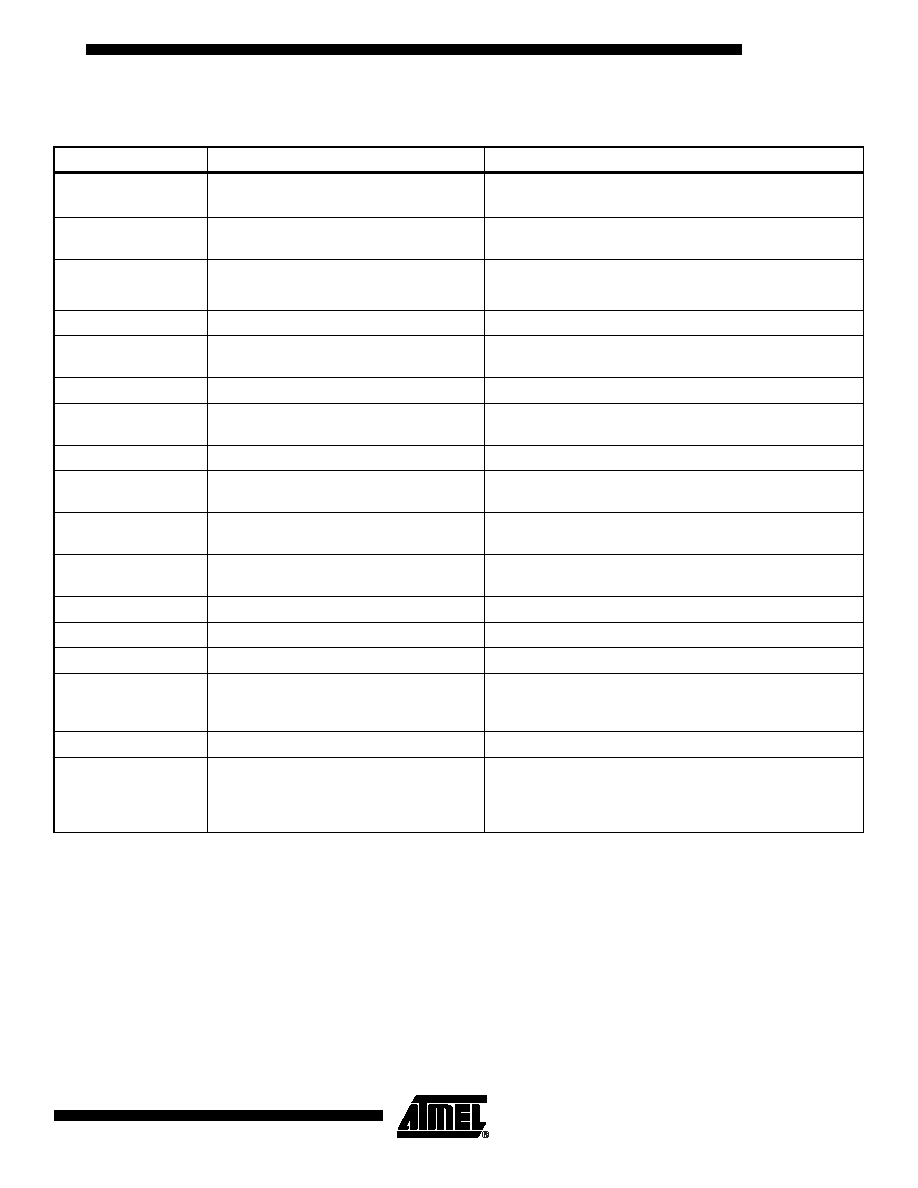
Table 8. TS8388BF/TS8388BFS Pin Description (CQFP68 package)
Symbol
Pin number
Function
GND
5, 13, 27, 28, 34, 35, 36, 41, 42, 43, 50, 51,
52, 53, 58, 59
Ground pins.
To be connected to external ground plane.
VPLUSD
1, 2, 16, 17, 18, 68
Digital positive supply (0V for ECL compatibility, 2.4V for
LVDS compatibility).(2)
V
CC
26, 29, 32, 33, 46, 47, 61
+5V positive supply.
VEE
30, 31, 44, 45, 48
-5V analog negative supply.
DVEE
8, 9, 10
-5V digital negative supply.
V
IN
54(1), 55
In phase (+) analog input signal of the Sample and Hold
differential preamplifier.
VINB
56, 57(1)
Inverted phase (-) of analog input signal (VIN).
CLK
37(1), 38
In phase (+) ECL clock input signal. The analog input is
sampled and held on the rising edge of the CLK signal.
CLKB
39, 40(1)
Inverted phase (-) of ECL clock input signal (CLK).
D0, D1, D2, D3, D4,
D5, D6, D7
23, 21, 19, 14, 6, 3, 66, 64
In phase (+) digital outputs.
B0 is the LSB. B7 is the MSB.
D0B, D1B, D2B, D3B,
D4B, D5B, D6B, D7B
24, 22, 20, 15, 7, 4, 67, 65
Inverted phase (-) digital outputs.
B0B is the inverted LSB. B7B is the inverted MSB.
OR
62
In phase (+) Out of Range Bit. Out of Range is high on the
leading edge of code 0 and code 256.
ORB
63
Inverted phase (+) Out of Range Bit (OR).
DR
11
In phase (+) output of Data Ready Signal.
DRB
12
Inverted phase (-) output of Data Ready Signal (DR).
GORB
25
Gray or Binary select output format control pin.
- Binary output format if GORB is floating or VCC.
- Gray output format if GORB is connected at ground (0V).
GAIN
60
ADC gain adjust pin.
DIOD/DRRB
49
This pin has a double function (can be left open or grounded
if not used):
- DIOD: die junction temperature monitoring pin.
- DRRB: asynchronous data ready reset function.
相關PDF資料 |
PDF描述 |
|---|---|
| TS8388BMFSB/T | 1-CH 8-BIT PROPRIETARY METHOD ADC, PARALLEL ACCESS, CQFP68 |
| TS8388BMFSB/Q | 1-CH 8-BIT PROPRIETARY METHOD ADC, PARALLEL ACCESS, CQFP68 |
| TS8388BMFB/Q | 1-CH 8-BIT PROPRIETARY METHOD ADC, PARALLEL ACCESS, CQFP68 |
| TS8388BMFSB/QNB1 | 1-CH 8-BIT PROPRIETARY METHOD ADC, PARALLEL ACCESS, CQFP68 |
| TS8388BMFSB/QNB2 | 1-CH 8-BIT PROPRIETARY METHOD ADC, PARALLEL ACCESS, CQFP68 |
相關代理商/技術參數 |
參數描述 |
|---|---|
| TS8388BMFS | 制造商:e2v technologies 功能描述:ADC 8-BIT 1 GSPS - Trays |
| TS8388BMFS9NB1 | 制造商:e2v technologies 功能描述:ADC 8-BIT 1 GSPS - Trays |
| TS8388BMFS9NB2 | 制造商:ATMEL 制造商全稱:ATMEL Corporation 功能描述:ADC 8-bit 1 GSPS |
| TS8388BMFS9NB3 | 制造商:ATMEL 制造商全稱:ATMEL Corporation 功能描述:ADC 8-bit 1 GSPS |
| TS8388BMFS9NC2 | 制造商:ATMEL 制造商全稱:ATMEL Corporation 功能描述:ADC 8-bit 1 GSPS |
發布緊急采購,3分鐘左右您將得到回復。