- 您現(xiàn)在的位置:買賣IC網(wǎng) > PDF目錄98299 > TS8388BVFSB/Q (ATMEL CORP) 2-CH 8-BIT PROPRIETARY METHOD ADC, PARALLEL ACCESS, CQFP68 PDF資料下載
參數(shù)資料
| 型號: | TS8388BVFSB/Q |
| 廠商: | ATMEL CORP |
| 元件分類: | ADC |
| 英文描述: | 2-CH 8-BIT PROPRIETARY METHOD ADC, PARALLEL ACCESS, CQFP68 |
| 封裝: | CERAMIC, QFP-68 |
| 文件頁數(shù): | 18/47頁 |
| 文件大小: | 1230K |
| 代理商: | TS8388BVFSB/Q |
第1頁第2頁第3頁第4頁第5頁第6頁第7頁第8頁第9頁第10頁第11頁第12頁第13頁第14頁第15頁第16頁第17頁當(dāng)前第18頁第19頁第20頁第21頁第22頁第23頁第24頁第25頁第26頁第27頁第28頁第29頁第30頁第31頁第32頁第33頁第34頁第35頁第36頁第37頁第38頁第39頁第40頁第41頁第42頁第43頁第44頁第45頁第46頁第47頁
25
TS8388BF
2144A–BDC–04/02
Data Ready Output
Signal Restart
The Data Ready output signal restarts on DRRB command rising edge, ECL logical high levels
(-0.8V). DRRB may also be Grounded, or is allowed to float, for normal free running Data
Ready output signal.
The Data Ready signal restart sequence depends on the logical level of the external encoding
clock, at DRRB rising edge instant:
The DRRB rising edge occurs when external encoding clock input (CLK, CLKB) is LOW:
The Data Ready output first rising edge occurs after half a clock period on the clock falling
edge, after a delay time TDR = 1320 ps already defined hereabove.
The DRRB rising edge occurs when external encoding clock input (CLK, CLKB) is HIGH:
The Data Ready output first rising edge occurs after one clock period on the clock falling
edge, and a delay TDR = 1320 ps.
Consequently, as the analog input is sampled on clock rising edge, the first digitized data cor-
responding to the first acquisition (N) after Data Ready signal restart (rising edge) is always
strobed by the third rising edge of the data ready signal.
The time delay (TD1) is specified between the last point of a change in the differential output
data (zero crossing point) to the rising or falling edge of the differential Data Ready signal (DR,
DRB) (zero crossing point).
For normal initialization of Data Ready output signal, the external encoding clock signal fre-
quency and level must be controlled. It is reminded that the minimum encoding clock sampling
rate for the ADC is 10 MSPS and consequently the clock cannot be stopped.
One single pin is used for both DRRB input command and die junction temperature monitor-
ing. Pin denomination will be DRRB/DIOD. On the former version denomination was DIOD.
Temperature monitoring and Data Ready control by DRRB is not possible simultaneously.
Analog Inputs (V
IN)
(V
INB)
The analog input Full Scale range is 0.5V peak to peak (Vpp), or -2 dBm into the 50
termina-
tion resistor.
In differential mode input configuration, that means 0.25V on each input, or ±125 mV around
0V. The input common mode is GROUND.
The typical input capacitance is 3 pF for TS8388B in CQFP package.
The input capacitance is mainly due to the package. The ESD protections are not connected
(but present) on the inputs.
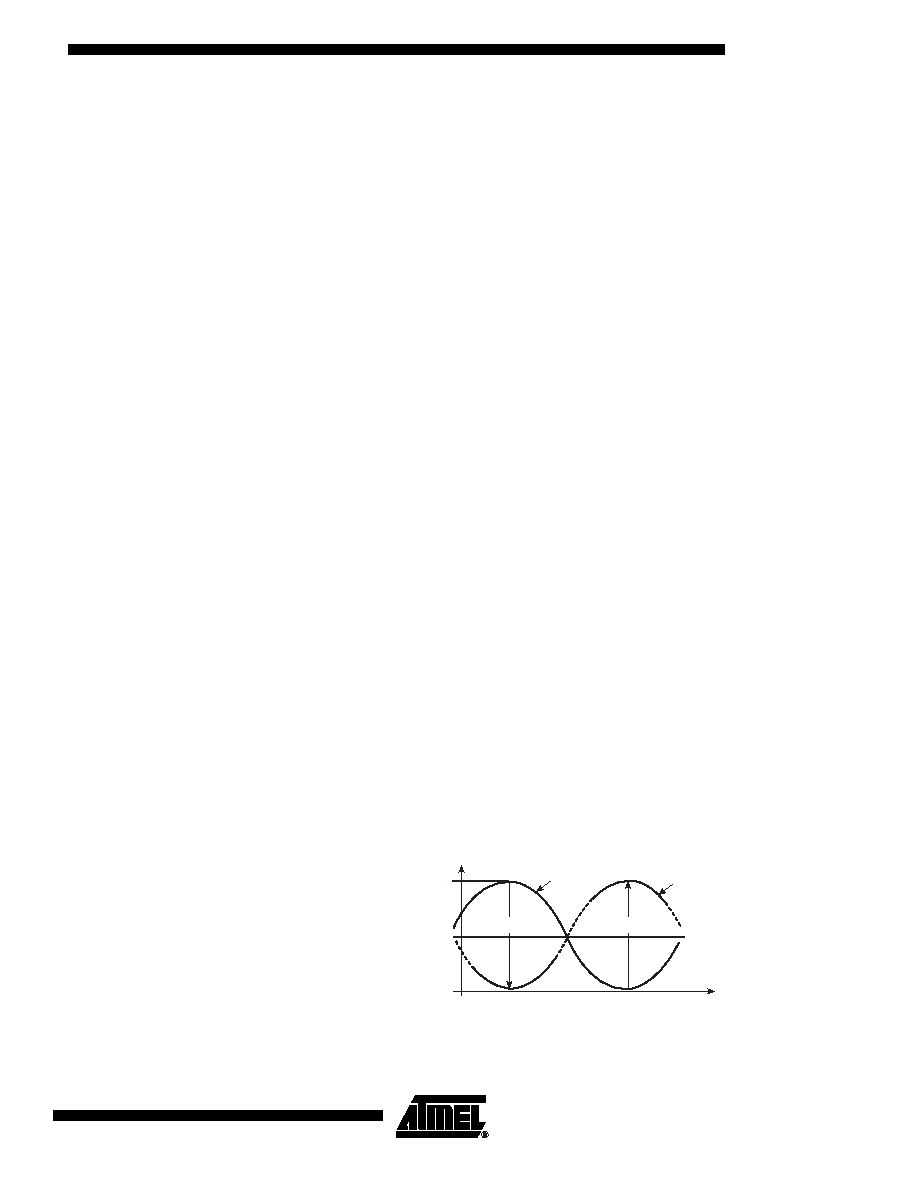
Differential Inputs
Voltage Span
Figure 27. Differiential Inputs Voltage Span
-125
125
[mV]
-250 mV
VIN
(VIN, VINB) =
±250 mV = 500 mV diff
500 mV
Full Scale
analog input
t
VINB
0V
250 mV
相關(guān)PDF資料 |
PDF描述 |
|---|---|
| TS8388BVFB/Q | 2-CH 8-BIT PROPRIETARY METHOD ADC, PARALLEL ACCESS, CQFP68 |
| TS8388BCFB/Q | 2-CH 8-BIT PROPRIETARY METHOD ADC, PARALLEL ACCESS, CQFP68 |
| TS8388BVFSB/Q | 2-CH 8-BIT PROPRIETARY METHOD ADC, PARALLEL ACCESS, CQFP68 |
| TS8388BCF | 1-CH 8-BIT PROPRIETARY METHOD ADC, PARALLEL ACCESS, CQFP68 |
| TS8388BMFB/Q | 1-CH 8-BIT PROPRIETARY METHOD ADC, PARALLEL ACCESS, CQFP68 |
相關(guān)代理商/技術(shù)參數(shù) |
參數(shù)描述 |
|---|---|
| TS8388BVGL | 制造商:e2v technologies 功能描述:ADC 8-BIT 1 GSPS - Trays |
| TS8388BVGL (+LID) | 制造商:e2v technologies 功能描述:ADC 8-BIT 1 GSPS - Trays |
| TS83C194 | 制造商:未知廠家 制造商全稱:未知廠家 功能描述:16-Bit Microcontroller |
| TS83C196KB-10 | 制造商:未知廠家 制造商全稱:未知廠家 功能描述:16-Bit Microcontroller |
| TS83C196KD | 制造商:未知廠家 制造商全稱:未知廠家 功能描述:Microcontroller |
發(fā)布緊急采購,3分鐘左右您將得到回復(fù)。