- 您現在的位置:買賣IC網 > PDF目錄363874 > W25Z040A (WINBOND ELECTRONICS CORP) 128K×36bit Pipeline ZWS(Zero-Wait-State) SRAM(128K×36位無等待時間的管線CMOS同步靜態RAM) PDF資料下載
參數資料
| 型號: | W25Z040A |
| 廠商: | WINBOND ELECTRONICS CORP |
| 英文描述: | 128K×36bit Pipeline ZWS(Zero-Wait-State) SRAM(128K×36位無等待時間的管線CMOS同步靜態RAM) |
| 中文描述: | 128K的× 36bit管道ZWS(零等待狀態)的SRAM(128K的× 36位無等待時間的管線的CMOS同步靜態內存) |
| 文件頁數: | 6/16頁 |
| 文件大小: | 136K |
| 代理商: | W25Z040A |
W25Z040A
- 6 -
Burst Mode Operation
Burst read or write is activated if ADV/LD = HIGH at the rising edge of CLK, where the new address
is composed of 2 new bits from burst counter and the remaining bits from the previous address. The
sequencing of the counter can be either linear if LBO = LOW or interleaved if LBO = HIGH.
CE
[3:1]
and
WE
controls are ignored during burst mode.
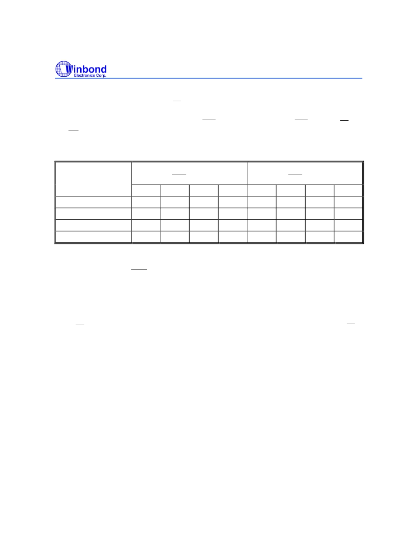
Burst Address Sequence
INTERLEAVED MODE
(LBO = V
DD
)
LINEAR MODE
(LBO = V
SS
)
A[1:0]
A[1:0]
A[1:0]
A[1:0]
A[1:0]
A[1:0]
A[1:0]
A[1:0]
External Start Address
00
01
10
11
00
01
10
11
Second Address
01
00
11
10
01
10
11
00
Third Address
10
11
00
01
10
11
00
01
Fourth Address
11
10
01
00
11
00
01
10
Stall Cycle
Stall cycle occurs when
CLKE
= HIGH is sampled. No internal clocks are generated. All addresses
and control signals are ignored. If the previous cycle is a READ, output remains the same. If the
previous cycle is a WRITE, output remains tri-stated. Any stall cycle will be added to increase the
latency of output and input data.
Unselect Cycle
When
CE
= HIGH is sampled, a unselect state is entered. Output is tri-stated. By setting ADV/LD =
HIGH for the following sampling cycle, the unselect state can be continued.
NOP Cycle
For a WRITE cycle with no asserted Byte-Write select signal, the device achieves a NOP operation.
No addresses will be sampled.
Power Down Mode
An asynchronous ZZ pin can be set High to force the device into a power down mode. Outputs will go
into High-Z state and the device draws only standby power. Minimum of 2 CLK cycles are required
after setting ZZ to High before the device is forced into power down operation. Any operation pending
when entering power down mode (read or write) is not guaranteed to successfully complete.
Therefore, ZZ mode must not be initiated until valid pending operations are completed. When exiting
ZZ mode during T
ZZR
, only the unselect or read cycle should be given while the SRAM will be waken
up again.
相關PDF資料 |
PDF描述 |
|---|---|
| W26010AJ-15 | 64K 16 HIGH-SPEED CMOS STATIC RAM |
| W26010AJ-151 | 64K 16 HIGH-SPEED CMOS STATIC RAM |
| W26010AJ-20 | 64K 16 HIGH-SPEED CMOS STATIC RAM |
| W26010AJ-25 | 64K 16 HIGH-SPEED CMOS STATIC RAM |
| W26010AT-15 | 64K 16 HIGH-SPEED CMOS STATIC RAM |
相關代理商/技術參數 |
參數描述 |
|---|---|
| W260 | 制造商:Leach International Corporation 功能描述:LEACH - W260 RELAY DATA SHEET - Bulk |
| W2600CR2 916028 | 制造商:Intel 功能描述:CROWN PASS 16DIMM DUAL NIC - Boxed Product (Development Kits) |
| W26010A | 制造商:WINBOND 制造商全稱:Winbond 功能描述:64K 16 HIGH-SPEED CMOS STATIC RAM |
| W26010AJ-15 | 制造商:WINBOND 制造商全稱:Winbond 功能描述:64K 16 HIGH-SPEED CMOS STATIC RAM |
| W26010AJ-151 | 制造商:WINBOND 制造商全稱:Winbond 功能描述:64K 16 HIGH-SPEED CMOS STATIC RAM |
發布緊急采購,3分鐘左右您將得到回復。