- 您現在的位置:買賣IC網 > PDF目錄21991 > XC2S15-5TQ144C (Xilinx Inc)IC FPGA 2.5V 96 CLB'S 144-PQFP PDF資料下載
參數資料
| 型號: | XC2S15-5TQ144C |
| 廠商: | Xilinx Inc |
| 文件頁數: | 3/99頁 |
| 文件大小: | 0K |
| 描述: | IC FPGA 2.5V 96 CLB'S 144-PQFP |
| 標準包裝: | 60 |
| 系列: | Spartan®-II |
| LAB/CLB數: | 96 |
| 邏輯元件/單元數: | 432 |
| RAM 位總計: | 16384 |
| 輸入/輸出數: | 86 |
| 門數: | 15000 |
| 電源電壓: | 2.375 V ~ 2.625 V |
| 安裝類型: | 表面貼裝 |
| 工作溫度: | 0°C ~ 85°C |
| 封裝/外殼: | 144-LQFP |
| 供應商設備封裝: | 144-TQFP(20x20) |
| 產品目錄頁面: | 599 (CN2011-ZH PDF) |
| 其它名稱: | 122-1218 XC2S15-5TQ144C-ND |
第1頁第2頁當前第3頁第4頁第5頁第6頁第7頁第8頁第9頁第10頁第11頁第12頁第13頁第14頁第15頁第16頁第17頁第18頁第19頁第20頁第21頁第22頁第23頁第24頁第25頁第26頁第27頁第28頁第29頁第30頁第31頁第32頁第33頁第34頁第35頁第36頁第37頁第38頁第39頁第40頁第41頁第42頁第43頁第44頁第45頁第46頁第47頁第48頁第49頁第50頁第51頁第52頁第53頁第54頁第55頁第56頁第57頁第58頁第59頁第60頁第61頁第62頁第63頁第64頁第65頁第66頁第67頁第68頁第69頁第70頁第71頁第72頁第73頁第74頁第75頁第76頁第77頁第78頁第79頁第80頁第81頁第82頁第83頁第84頁第85頁第86頁第87頁第88頁第89頁第90頁第91頁第92頁第93頁第94頁第95頁第96頁第97頁第98頁第99頁
Spartan-II FPGA Family: Functional Description
DS001-2 (v2.8) June 13, 2008
Module 2 of 4
Product Specification
11
R
Similarly, the F6 multiplexer combines the outputs of all four
function generators in the CLB by selecting one of the
F5-multiplexer outputs. This permits the implementation of
any 6-input function, an 8:1 multiplexer, or selected
functions of up to 19 inputs.
Each CLB has four direct feedthrough paths, one per LC.
These paths provide extra data input lines or additional
local routing that does not consume logic resources.
Arithmetic Logic
Dedicated carry logic provides capability for high-speed
arithmetic functions. The Spartan-II FPGA CLB supports
two separate carry chains, one per slice. The height of the
carry chains is two bits per CLB.
The arithmetic logic includes an XOR gate that allows a
1-bit full adder to be implemented within an LC. In addition,
a dedicated AND gate improves the efficiency of multiplier
implementation.
The dedicated carry path can also be used to cascade
function generators for implementing wide logic functions.
BUFTs
Each Spartan-II FPGA CLB contains two 3-state drivers
(BUFTs) that can drive on-chip busses. See "Dedicated
Routing," page 12. Each Spartan-II FPGA BUFT has an
independent 3-state control pin and an independent input
pin.
Block RAM
Spartan-II FPGAs incorporate several large block RAM
memories. These complement the distributed RAM
Look-Up Tables (LUTs) that provide shallow memory
structures implemented in CLBs.
Block RAM memory blocks are organized in columns. All
Spartan-II devices contain two such columns, one along
each vertical edge. These columns extend the full height of
the chip. Each memory block is four CLBs high, and
consequently, a Spartan-II device eight CLBs high will
contain two memory blocks per column, and a total of four
blocks.
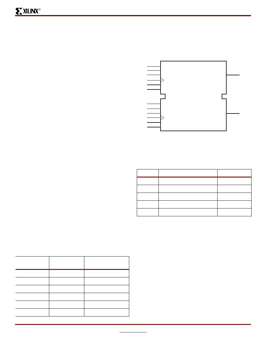
Each block RAM cell, as illustrated in Figure 5, is a fully
synchronous dual-ported 4096-bit RAM with independent
control signals for each port. The data widths of the two
ports can be configured independently, providing built-in
bus-width conversion.
Table 6 shows the depth and width aspect ratios for the
block RAM.
The Spartan-II FPGA block RAM also includes dedicated
routing to provide an efficient interface with both CLBs and
other block RAMs.
Programmable Routing Matrix
It is the longest delay path that limits the speed of any
worst-case design. Consequently, the Spartan-II routing
architecture and its place-and-route software were defined
in a single optimization process. This joint optimization
minimizes long-path delays, and consequently, yields the
best system performance.
The joint optimization also reduces design compilation
times because the architecture is software-friendly. Design
cycles are correspondingly reduced due to shorter design
iteration times.
Table 5: Spartan-II Block RAM Amounts
Spartan-II
Device
# of Blocks
Total Block RAM
Bits
XC2S15
4
16K
XC2S30
6
24K
XC2S50
8
32K
XC2S100
10
40K
XC2S150
12
48K
XC2S200
14
56K
Figure 5: Dual-Port Block RAM
Table 6: Block RAM Port Aspect Ratios
Width
Depth
ADDR Bus
Data Bus
1
4096
ADDR<11:0>
DATA<0>
2
2048
ADDR<10:0>
DATA<1:0>
4
1024
ADDR<9:0>
DATA<3:0>
8
512
ADDR<8:0>
DATA<7:0>
16
256
ADDR<7:0>
DATA<15:0>
WEB
ENB
RSTB
CLKB
ADDRB[#:0]
DIB[#:0]
WEA
ENA
RSTA
CLKA
ADD[#:0]
DIA[#:0]
DOA[#:0]
DOB[#:0]
RAMB4_S#_S#
DS001_05_060100
相關PDF資料 |
PDF描述 |
|---|---|
| VE-J6F-CW | CONVERTER MOD DC/DC 72V 100W |
| MAX1617AMEE | IC TEMP SENSOR SMBUS SRL 16-QSOP |
| GBM18DSEI-S243 | CONN EDGECARD 36POS .156 EYELET |
| VE-J60-CW | CONVERTER MOD DC/DC 5V 100W |
| VJ1206A471KBEAT4X | CAP CER 470PF 500V 10% NP0 1206 |
相關代理商/技術參數 |
參數描述 |
|---|---|
| XC2S15-5TQ144I | 功能描述:IC FPGA 2.5V I-TEMP 144-TQFP RoHS:否 類別:集成電路 (IC) >> 嵌入式 - FPGA(現場可編程門陣列) 系列:Spartan®-II 標準包裝:40 系列:Spartan® 6 LX LAB/CLB數:3411 邏輯元件/單元數:43661 RAM 位總計:2138112 輸入/輸出數:358 門數:- 電源電壓:1.14 V ~ 1.26 V 安裝類型:表面貼裝 工作溫度:-40°C ~ 100°C 封裝/外殼:676-BGA 供應商設備封裝:676-FBGA(27x27) |
| XC2S15-5TQG144C | 制造商:Xilinx 功能描述:FPGA SPARTAN-II 15K GATES 432 CELLS 263MHZ 2.5V 144TQFP EP - Trays 制造商:Xilinx 功能描述:IC SYSTEM GATE 制造商:Xilinx 功能描述:XC2S15-5TQG144C |
| XC2S15-5TQG144I | 制造商:Xilinx 功能描述:IC SYSTEM GATE 制造商:Xilinx 功能描述:FPGA SPARTAN-II 15K GATES 432 CELLS 263MHZ 2.5V 144TQFP EP - Trays |
| XC2S15-5VQ100C | 功能描述:IC FPGA 2.5V 96 CLB'S 100-VQFP RoHS:否 類別:集成電路 (IC) >> 嵌入式 - FPGA(現場可編程門陣列) 系列:Spartan®-II 標準包裝:40 系列:Spartan® 6 LX LAB/CLB數:3411 邏輯元件/單元數:43661 RAM 位總計:2138112 輸入/輸出數:358 門數:- 電源電壓:1.14 V ~ 1.26 V 安裝類型:表面貼裝 工作溫度:-40°C ~ 100°C 封裝/外殼:676-BGA 供應商設備封裝:676-FBGA(27x27) |
| XC2S15-5VQ100I | 功能描述:IC FPGA 2.5V I-TEMP 100-VQFP RoHS:否 類別:集成電路 (IC) >> 嵌入式 - FPGA(現場可編程門陣列) 系列:Spartan®-II 標準包裝:40 系列:Spartan® 6 LX LAB/CLB數:3411 邏輯元件/單元數:43661 RAM 位總計:2138112 輸入/輸出數:358 門數:- 電源電壓:1.14 V ~ 1.26 V 安裝類型:表面貼裝 工作溫度:-40°C ~ 100°C 封裝/外殼:676-BGA 供應商設備封裝:676-FBGA(27x27) |
發布緊急采購,3分鐘左右您將得到回復。