- 您現(xiàn)在的位置:買賣IC網(wǎng) > PDF目錄21991 > XC2S30-5VQG100C (Xilinx Inc)IC FPGA 2.5V 216 CLB'S 100-VQFP PDF資料下載
參數(shù)資料
| 型號: | XC2S30-5VQG100C |
| 廠商: | Xilinx Inc |
| 文件頁數(shù): | 17/99頁 |
| 文件大小: | 0K |
| 描述: | IC FPGA 2.5V 216 CLB'S 100-VQFP |
| 標準包裝: | 90 |
| 系列: | Spartan®-II |
| LAB/CLB數(shù): | 216 |
| 邏輯元件/單元數(shù): | 972 |
| RAM 位總計: | 24576 |
| 輸入/輸出數(shù): | 60 |
| 門數(shù): | 30000 |
| 電源電壓: | 2.375 V ~ 2.625 V |
| 安裝類型: | 表面貼裝 |
| 工作溫度: | 0°C ~ 85°C |
| 封裝/外殼: | 100-TQFP |
| 供應商設備封裝: | 100-VQFP(14x14) |
| 產(chǎn)品目錄頁面: | 599 (CN2011-ZH PDF) |
| 其它名稱: | 122-1513-5 |
第1頁第2頁第3頁第4頁第5頁第6頁第7頁第8頁第9頁第10頁第11頁第12頁第13頁第14頁第15頁第16頁當前第17頁第18頁第19頁第20頁第21頁第22頁第23頁第24頁第25頁第26頁第27頁第28頁第29頁第30頁第31頁第32頁第33頁第34頁第35頁第36頁第37頁第38頁第39頁第40頁第41頁第42頁第43頁第44頁第45頁第46頁第47頁第48頁第49頁第50頁第51頁第52頁第53頁第54頁第55頁第56頁第57頁第58頁第59頁第60頁第61頁第62頁第63頁第64頁第65頁第66頁第67頁第68頁第69頁第70頁第71頁第72頁第73頁第74頁第75頁第76頁第77頁第78頁第79頁第80頁第81頁第82頁第83頁第84頁第85頁第86頁第87頁第88頁第89頁第90頁第91頁第92頁第93頁第94頁第95頁第96頁第97頁第98頁第99頁
Spartan-II FPGA Family: Functional Description
DS001-2 (v2.8) June 13, 2008
Module 2 of 4
Product Specification
24
R
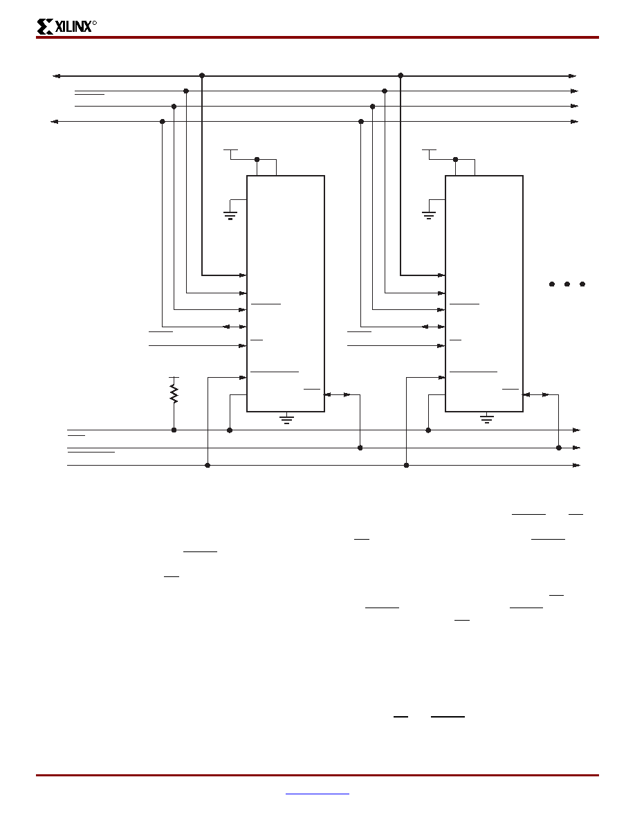
Multiple Spartan-II FPGAs can be configured using the
Slave Parallel mode, and be made to start-up
simultaneously. To configure multiple devices in this way,
wire the individual CCLK, Data, WRITE, and BUSY pins of
all the devices in parallel. The individual devices are loaded
separately by asserting the CS pin of each device in turn
and writing the appropriate data. Sync-to-DONE start-up
timing is used to ensure that the start-up sequence does not
begin until all the FPGAs have been loaded. See "Start-up,"
Write
When using the Slave Parallel Mode, write operations send
packets of byte-wide configuration data into the FPGA.
Figure 19, page 25 shows a flowchart of the write sequence
used to load data into the Spartan-II FPGA. This is an
expansion of the "Load Configuration Data Frames" block in
Figure 11, page 18. The timing for write operations is shown
For the present example, the user holds WRITE and CS
Low throughout the sequence of write operations. Note that
when CS is asserted on successive CCLKs, WRITE must
remain either asserted or de-asserted. Otherwise an abort
will be initiated, as in the next section.
1.
Drive data onto D0-D7. Note that to avoid contention,
the data source should not be enabled while CS is Low
and WRITE is High. Similarly, while WRITE is High, no
more than one device’s CS should be asserted.
2.
On the rising edge of CCLK: If BUSY is Low, the data is
accepted on this clock. If BUSY is High (from a previous
write), the data is not accepted. Acceptance will instead
occur on the first clock after BUSY goes Low, and the
data must be held until this happens.
3.
Repeat steps 1 and 2 until all the data has been sent.
4.
De-assert CS and WRITE.
Figure 18: Slave Parallel Configuration Circuit Diagram
M1 M2
M0
D0:D7
CCLK
WRITE
BUSY
CS
PROGRAM
DONEINIT
CCLK
DATA[7:0]
WRITE
BUSY
CS(0)
330
Ω
Spartan-II
FPGA
DONE
INIT
PROGRAM
M1 M2
M0
D0:D7
CCLK
WRITE
BUSY
CS
PROGRAM
DONEINIT
CS(1)
Spartan-II
FPGA
DS001_18_060608
GND
相關PDF資料 |
PDF描述 |
|---|---|
| VI-27L-CW-F2 | CONVERTER MOD DC/DC 28V 100W |
| XC3S50AN-4TQG144C | IC SPARTAN-3AN FPGA 50K 144TQFP |
| XC3S50A-4FTG256C | IC SPARTAN-3A FPGA 50K 256FTBGA |
| VI-B5D-CX | CONVERTER MOD DC/DC 85V 75W |
| VI-27K-CW-F4 | CONVERTER MOD DC/DC 40V 100W |
相關代理商/技術參數(shù) |
參數(shù)描述 |
|---|---|
| XC2S30-5VQG100I | 制造商:Xilinx 功能描述:FPGA SPARTAN-II 30K GATES 972 CELLS 263MHZ 2.5V 100VTQFP - Trays 制造商:Xilinx 功能描述:IC SYSTEM GATE |
| XC2S30-6CS144C | 功能描述:IC FPGA 2.5V C-TEMP 144-CSBGA RoHS:否 類別:集成電路 (IC) >> 嵌入式 - FPGA(現(xiàn)場可編程門陣列) 系列:Spartan®-II 標準包裝:40 系列:Spartan® 6 LX LAB/CLB數(shù):3411 邏輯元件/單元數(shù):43661 RAM 位總計:2138112 輸入/輸出數(shù):358 門數(shù):- 電源電壓:1.14 V ~ 1.26 V 安裝類型:表面貼裝 工作溫度:-40°C ~ 100°C 封裝/外殼:676-BGA 供應商設備封裝:676-FBGA(27x27) |
| XC2S30-6CS144I | 制造商:XILINX 制造商全稱:XILINX 功能描述:Spartan-II 2.5V FPGA Family:Introduction and Ordering Information |
| XC2S30-6CSG144C | 制造商:Xilinx 功能描述:FPGA SPARTAN-II 30K GATES 972 CELLS 263MHZ 2.5V 144CSBGA - Trays |
| XC2S30-6CSG144I | 制造商:XILINX 制造商全稱:XILINX 功能描述:Spartan-II FPGA Family |
發(fā)布緊急采購,3分鐘左右您將得到回復。