- 您現在的位置:買賣IC網 > PDF目錄21987 > XC3S500E-4CPG132C (Xilinx Inc)IC SPARTAN-3E FPGA 500K 132CSBGA PDF資料下載
參數資料
| 型號: | XC3S500E-4CPG132C |
| 廠商: | Xilinx Inc |
| 文件頁數: | 146/227頁 |
| 文件大小: | 0K |
| 描述: | IC SPARTAN-3E FPGA 500K 132CSBGA |
| 產品培訓模塊: | FPGAs Spartan3 |
| 標準包裝: | 360 |
| 系列: | Spartan®-3E |
| LAB/CLB數: | 1164 |
| 邏輯元件/單元數: | 10476 |
| RAM 位總計: | 368640 |
| 輸入/輸出數: | 92 |
| 門數: | 500000 |
| 電源電壓: | 1.14 V ~ 1.26 V |
| 安裝類型: | 表面貼裝 |
| 工作溫度: | 0°C ~ 85°C |
| 封裝/外殼: | 132-TFBGA,CSPBGA |
| 供應商設備封裝: | 132-CSPBGA(8x8) |
| 配用: | 122-1536-ND - KIT STARTER SPARTAN-3E |
| 其它名稱: | 122-1484 |
第1頁第2頁第3頁第4頁第5頁第6頁第7頁第8頁第9頁第10頁第11頁第12頁第13頁第14頁第15頁第16頁第17頁第18頁第19頁第20頁第21頁第22頁第23頁第24頁第25頁第26頁第27頁第28頁第29頁第30頁第31頁第32頁第33頁第34頁第35頁第36頁第37頁第38頁第39頁第40頁第41頁第42頁第43頁第44頁第45頁第46頁第47頁第48頁第49頁第50頁第51頁第52頁第53頁第54頁第55頁第56頁第57頁第58頁第59頁第60頁第61頁第62頁第63頁第64頁第65頁第66頁第67頁第68頁第69頁第70頁第71頁第72頁第73頁第74頁第75頁第76頁第77頁第78頁第79頁第80頁第81頁第82頁第83頁第84頁第85頁第86頁第87頁第88頁第89頁第90頁第91頁第92頁第93頁第94頁第95頁第96頁第97頁第98頁第99頁第100頁第101頁第102頁第103頁第104頁第105頁第106頁第107頁第108頁第109頁第110頁第111頁第112頁第113頁第114頁第115頁第116頁第117頁第118頁第119頁第120頁第121頁第122頁第123頁第124頁第125頁第126頁第127頁第128頁第129頁第130頁第131頁第132頁第133頁第134頁第135頁第136頁第137頁第138頁第139頁第140頁第141頁第142頁第143頁第144頁第145頁當前第146頁第147頁第148頁第149頁第150頁第151頁第152頁第153頁第154頁第155頁第156頁第157頁第158頁第159頁第160頁第161頁第162頁第163頁第164頁第165頁第166頁第167頁第168頁第169頁第170頁第171頁第172頁第173頁第174頁第175頁第176頁第177頁第178頁第179頁第180頁第181頁第182頁第183頁第184頁第185頁第186頁第187頁第188頁第189頁第190頁第191頁第192頁第193頁第194頁第195頁第196頁第197頁第198頁第199頁第200頁第201頁第202頁第203頁第204頁第205頁第206頁第207頁第208頁第209頁第210頁第211頁第212頁第213頁第214頁第215頁第216頁第217頁第218頁第219頁第220頁第221頁第222頁第223頁第224頁第225頁第226頁第227頁
Spartan-3E FPGA Family: Functional Description
DS312 (v4.1) July 19, 2013
Product Specification
25
Main Logic Paths
Central to the operation of each slice are two nearly
identical data paths at the top and bottom of the slice. The
description that follows uses names associated with the
bottom path. (The top path names appear in parentheses.)
The basic path originates at an interconnect switch matrix
outside the CLB. See Interconnect for more information on
the switch matrix and the routing connections.
Four lines, F1 through F4 (or G1 through G4 on the upper
path), enter the slice and connect directly to the LUT. Once
inside the slice, the lower 4-bit path passes through a LUT
‘F’ (or ‘G’) that performs logic operations. The LUT Data
output, ‘D’, offers five possible paths:
1.
Exit the slice via line “X” (or “Y”) and return to
interconnect.
2.
Inside the slice, “X” (or “Y”) serves as an input to the
DXMUX (or DYMUX) which feeds the data input, “D”, of
the FFX (or FFY) storage element. The “Q” output of the
storage element drives the line XQ (or YQ) which exits
the slice.
3.
Control the CYMUXF (or CYMUXG) multiplexer on the
carry chain.
4.
With the carry chain, serve as an input to the XORF (or
XORG) exclusive-OR gate that performs arithmetic
operations, producing a result on “X” (or “Y”).
5.
Drive the multiplexer F5MUX to implement logic
functions wider than four bits. The “D” outputs of both
the F-LUT and G-LUT serve as data inputs to this
multiplexer.
In addition to the main logic paths described above, there
are two bypass paths that enter the slice as BX and BY.
Once inside the FPGA, BX in the bottom half of the slice (or
BY in the top half) can take any of several possible
branches:
1.
Bypass both the LUT and the storage element, and
then exit the slice as BXOUT (or BYOUT) and return to
interconnect.
2.
Bypass the LUT, and then pass through a storage
element via the D input before exiting as XQ (or YQ).
3.
Control the wide function multiplexer F5MUX (or
FiMUX).
4.
Via multiplexers, serve as an input to the carry chain.
5.
Drive the DI input of the LUT.
6.
BY can control the REV inputs of both the FFY and FFX
storage elements. See Storage Element Functions.
7.
Finally, the DIG_MUX multiplexer can switch BY onto
the DIG line, which exits the slice.
The control inputs CLK, CE, SR, BX and BY have
programmable polarity. The LUT inputs do not need
programmable polarity because their function can be
inverted inside the LUT.
The sections that follow provide more detail on individual
functions of the slice.
Look-Up Tables
The Look-Up Table or LUT is a RAM-based function
generator and is the main resource for implementing logic
functions. Furthermore, the LUTs in each SLICEM pair can
be configured as Distributed RAM or a 16-bit shift register,
as described later.
Each of the two LUTs (F and G) in a slice have four logic
inputs (A1-A4) and a single output (D). Any four-variable
Boolean logic operation can be implemented in one LUT.
Functions with more inputs can be implemented by
cascading LUTs or by using the wide function multiplexers
that are described later.
The output of the LUT can connect to the wide multiplexer
logic, the carry and arithmetic logic, or directly to a CLB
output or to the CLB storage element. See Figure 18.
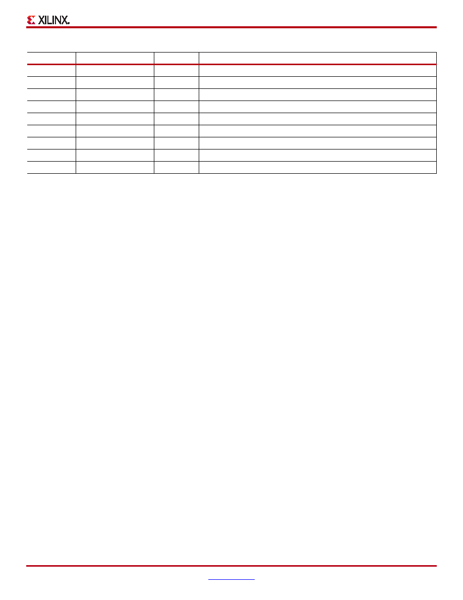
SHIFTOUT
SLICEM Bottom
Output
Shift data output from F-LUT RAM
CIN
SLICEL/M Bottom
Input
Carry chain input
COUT
SLICEL/M Top
Output
Carry chain output
X
SLICEL/M Bottom
Output
Combinatorial output
Y
SLICEL/M Top
Output
Combinatorial output
XB
SLICEL/M Bottom
Output
Combinatorial output from carry or F-LUT SRL16 (SLICEM)
YB
SLICEL/M Top
Output
Combinatorial output from carry or G-LUT SRL16 (SLICEM)
XQ
SLICEL/M Bottom
Output
FFX output
YQ
SLICEL/M Top
Output
FFY output
Table 10: Slice Inputs and Outputs (Cont’d)
Name
Location
Direction
Description
相關PDF資料 |
PDF描述 |
|---|---|
| HMM06DRUH | CONN EDGECARD 12POS .156 DIP SLD |
| MAX6627MKA#T | IC TEMP SENSOR DGTL SOT23-8 |
| LM75BIMMX-5+ | IC TEMP SENSOR WATCHDOG 8MSOP |
| LM75BIMMX-3+ | IC TEMP SENSOR WATCHDOG 8MSOP |
| GBB15DHRN | CONN CARD EXTEND 30POS .050" SLD |
相關代理商/技術參數 |
參數描述 |
|---|---|
| XC3S500E-4CPG132I | 功能描述:IC FPGA SPARTAN-3E 500K 132CSBGA RoHS:是 類別:集成電路 (IC) >> 嵌入式 - FPGA(現場可編程門陣列) 系列:Spartan®-3E 標準包裝:40 系列:Spartan® 6 LX LAB/CLB數:3411 邏輯元件/單元數:43661 RAM 位總計:2138112 輸入/輸出數:358 門數:- 電源電壓:1.14 V ~ 1.26 V 安裝類型:表面貼裝 工作溫度:-40°C ~ 100°C 封裝/外殼:676-BGA 供應商設備封裝:676-FBGA(27x27) |
| XC3S500E-4CPG132I4124 | 制造商:Xilinx 功能描述: |
| XC3S500E-4FG320C | 制造商:Xilinx 功能描述:FPGA SPARTAN-3E 500K GATES 10476 CELLS 572MHZ 90NM 1.2V 320F - Trays |
| XC3S500E-4FG320I | 功能描述:IC FPGA SPARTAN 3E 320FBGA RoHS:否 類別:集成電路 (IC) >> 嵌入式 - FPGA(現場可編程門陣列) 系列:Spartan®-3E 標準包裝:40 系列:Spartan® 6 LX LAB/CLB數:3411 邏輯元件/單元數:43661 RAM 位總計:2138112 輸入/輸出數:358 門數:- 電源電壓:1.14 V ~ 1.26 V 安裝類型:表面貼裝 工作溫度:-40°C ~ 100°C 封裝/外殼:676-BGA 供應商設備封裝:676-FBGA(27x27) |
| XC3S500E-4FGG320C | 功能描述:IC SPARTAN-3E FPGA 500K 320FBGA RoHS:是 類別:集成電路 (IC) >> 嵌入式 - FPGA(現場可編程門陣列) 系列:Spartan®-3E 標準包裝:60 系列:XP LAB/CLB數:- 邏輯元件/單元數:10000 RAM 位總計:221184 輸入/輸出數:244 門數:- 電源電壓:1.71 V ~ 3.465 V 安裝類型:表面貼裝 工作溫度:0°C ~ 85°C 封裝/外殼:388-BBGA 供應商設備封裝:388-FPBGA(23x23) 其它名稱:220-1241 |
發布緊急采購,3分鐘左右您將得到回復。