- 您現在的位置:買賣IC網 > PDF目錄164976 > A40MX04-FPL44 FPGA, 547 CLBS, 6000 GATES, 48 MHz, PQCC44 PDF資料下載
參數資料
| 型號: | A40MX04-FPL44 |
| 元件分類: | FPGA |
| 英文描述: | FPGA, 547 CLBS, 6000 GATES, 48 MHz, PQCC44 |
| 封裝: | PLASTIC, LCC-44 |
| 文件頁數: | 24/124頁 |
| 文件大小: | 3142K |
| 代理商: | A40MX04-FPL44 |
第1頁第2頁第3頁第4頁第5頁第6頁第7頁第8頁第9頁第10頁第11頁第12頁第13頁第14頁第15頁第16頁第17頁第18頁第19頁第20頁第21頁第22頁第23頁當前第24頁第25頁第26頁第27頁第28頁第29頁第30頁第31頁第32頁第33頁第34頁第35頁第36頁第37頁第38頁第39頁第40頁第41頁第42頁第43頁第44頁第45頁第46頁第47頁第48頁第49頁第50頁第51頁第52頁第53頁第54頁第55頁第56頁第57頁第58頁第59頁第60頁第61頁第62頁第63頁第64頁第65頁第66頁第67頁第68頁第69頁第70頁第71頁第72頁第73頁第74頁第75頁第76頁第77頁第78頁第79頁第80頁第81頁第82頁第83頁第84頁第85頁第86頁第87頁第88頁第89頁第90頁第91頁第92頁第93頁第94頁第95頁第96頁第97頁第98頁第99頁第100頁第101頁第102頁第103頁第104頁第105頁第106頁第107頁第108頁第109頁第110頁第111頁第112頁第113頁第114頁第115頁第116頁第117頁第118頁第119頁第120頁第121頁第122頁第123頁第124頁
40MX and 42MX FPGA Families
1- 6
v6.1
MultiPlex I/O Modules
42MX devices feature Multiplex I/Os and support 5.0V,
3.3V, and mixed 3.3V/5.0V operations.
The MultiPlex I/O modules provide the interface between
the device pins and the logic array. Figure 1-9 is a block
diagram of the 42MX I/O module. A variety of user
functions, determined by a library macro selection, can
be implemented in the module. (Refer to the Antifuse
Macro Library Guide for more information.) All 42MX I/O
modules contain tristate buffers, with input and output
latches that can be configured for input, output, or
bidirectional operation.
All 42MX devices contain flexible I/O structures, where
each output pin has a dedicated output-enable control
(Figure 1-9). The I/O module can be used to latch input or
output data, or both, providing fast set-up time. In
addition, the Actel Designer software tools can build a D-
type flip-flop using a C-module combined with an I/O
module to register input and output signals. Refer to the
Antifuse Macro Library Guide for more details.
A42MX24 and A42MX36 devices also offer selectable PCI
output drives, enabling 100% compliance with version
2.1 of the PCI specification. For low-power systems, all
inputs and outputs are turned off to reduce current
consumption to below 500
μA.
To achieve 5.0V or 3.3V PCI-compliant output drives on
A42MX24 and A42MX36 devices, a chip-wide PCI fuse is
programmed via the Device Selection Wizard in the
Designer software (Figure 1-10). When the PCI fuse is not
programmed, the output drive is standard.
Actel's Designer software development tools provide a
design library of I/O macro functions that can implement
all I/O configurations supported by the MX FPGAs.
Other Architectural Features
Performance
MX devices can operate with internal clock frequencies
of 250 MHz, enabling fast execution of complex logic
functions. MX devices are live on power-up and do not
require auxiliary configuration devices and thus are an
optimal
platform
to
integrate
the
functionality
contained in multiple programmable logic devices. In
addition, designs that previously would have required a
gate array to meet performance can be integrated into
an MX device with improvements in cost and time-to-
market. Using timing-driven place-and-route (TDPR)
tools, designers can achieve highly deterministic device
performance.
User Security
The Actel FuseLock provides robust security against
design theft. Special security fuses are hidden in the
fabric of the device and prevent unauthorized users from
accessing the programming and/or probe interfaces. It is
virtually impossible to identify or bypass these fuses
without damaging the device, making Actel antifuse
FPGAs immune to both invasive and noninvasive attacks.
Special security fuses in 40MX devices include the Probe
Fuse and Program Fuse. The former disables the probing
circuitry while the latter prohibits further programming
of all fuses, including the Probe Fuse. In 42MX devices,
there is the Security Fuse which, when programmed,
both disables the probing circuitry and prohibits further
programming of the device.
Look for this symbol to ensure your valuable IP is secure.
Security in Actel Antifuse FPGAs application note.
Note: *Can be configured as a Latch or D Flip-Flop (Using
C-Module)
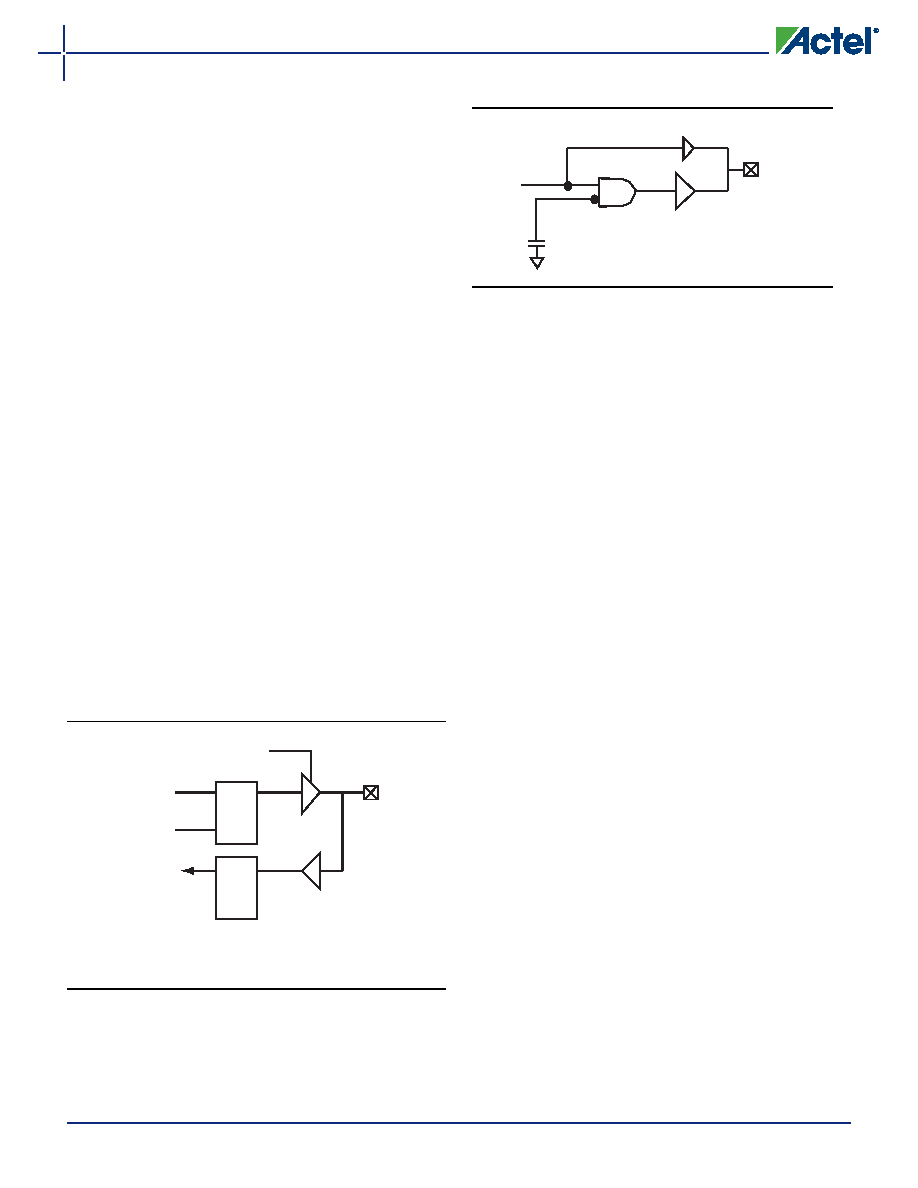
Figure 1-9 42MX I/O Module
Q
D
From Array
To Array
G/CLK*
Q
D
PAD
EN
Figure 1-10 PCI Output Structure of A42MX24 and
A42MX36 Devices
Signal
PCI Enable
PCI
Fuse
Drive
STD
Output
相關PDF資料 |
PDF描述 |
|---|---|
| A40MX04-FPL68X79 | FPGA, 547 CLBS, 6000 GATES, 48 MHz, PQCC68 |
| A40MX04-FPL68 | FPGA, 547 CLBS, 6000 GATES, 48 MHz, PQCC68 |
| A40MX04-FPL84X79 | FPGA, 547 CLBS, 6000 GATES, 48 MHz, PQCC84 |
| A40MX04-FPL84 | FPGA, 547 CLBS, 6000 GATES, 48 MHz, PQCC84 |
| A40MX04-FPQ100X79 | FPGA, 547 CLBS, 6000 GATES, 48 MHz, PQFP100 |
相關代理商/技術參數 |
參數描述 |
|---|---|
| A40MX04-FPL44I | 制造商:未知廠家 制造商全稱:未知廠家 功能描述:Field Programmable Gate Array (FPGA) |
| A40MX04-FPL44M | 制造商:未知廠家 制造商全稱:未知廠家 功能描述:Field Programmable Gate Array (FPGA) |
| A40MX04-FPL68 | 功能描述:IC FPGA MX SGL CHIP 6K 68-PLCC RoHS:否 類別:集成電路 (IC) >> 嵌入式 - FPGA(現場可編程門陣列) 系列:MX 標準包裝:152 系列:IGLOO PLUS LAB/CLB數:- 邏輯元件/單元數:792 RAM 位總計:- 輸入/輸出數:120 門數:30000 電源電壓:1.14 V ~ 1.575 V 安裝類型:表面貼裝 工作溫度:-40°C ~ 85°C 封裝/外殼:289-TFBGA,CSBGA 供應商設備封裝:289-CSP(14x14) |
| A40MX04-FPL68I | 制造商:未知廠家 制造商全稱:未知廠家 功能描述:Field Programmable Gate Array (FPGA) |
| A40MX04-FPL68M | 制造商:未知廠家 制造商全稱:未知廠家 功能描述:Field Programmable Gate Array (FPGA) |
發布緊急采購,3分鐘左右您將得到回復。