- 您現在的位置:買賣IC網 > PDF目錄373911 > AD7654AST (ANALOG DEVICES INC) Dual 2-Channel Simultaneous Sampling SAR 500 kSPS 16-Bit ADC PDF資料下載
參數資料
| 型號: | AD7654AST |
| 廠商: | ANALOG DEVICES INC |
| 元件分類: | ADC |
| 英文描述: | Dual 2-Channel Simultaneous Sampling SAR 500 kSPS 16-Bit ADC |
| 中文描述: | 4-CH 16-BIT SUCCESSIVE APPROXIMATION ADC, SERIAL/PARALLEL ACCESS, PQFP48 |
| 封裝: | MS-026-BBC, LQFP-48 |
| 文件頁數: | 12/24頁 |
| 文件大小: | 734K |
| 代理商: | AD7654AST |
REV. 0
–12–
AD7654
CIRCUIT INFORMATION
The AD7654 is a very fast, low power, single-supply, precise
simultaneous sampling 16-bit analog-to-digital converter (ADC).
The AD7654 provides the user with two on-chip track-and-hold,
successive approximation ADCs that do not exhibit any pipeline
or latency, making it ideal for multiple multiplexed channel
applications. The AD7654 can be also used as a 4-channel ADC
with two pairs simultaneously sampled.
The AD7654 can be operated from a single 5 V supply and be
interfaced to either 5 V or 3 V digital logic. It is housed in
48-lead LQFP or tiny 48-lead LFCSP packages that combine
space savings and allow flexible configurations as either a serial
or parallel interface. The AD7654 is pin-to-pin-compatible with
PulSAR ADCs.
Modes of Operation
The AD7654 features two modes of operation, Normal and
Impulse. Each of these modes is more suitable for specific
applications.
The Normal Mode is the fastest mode (500 kSPS). Except when it
is powered down (PD HIGH), the power dissipation is almost
independent of the sampling rate.
The Impulse Mode, the lowest power dissipation mode, allows
power saving between conversions. The maximum throughput
in this mode is 444 kSPS. When operating at 10 kSPS, for
example, it typically consumes only 2.6 mW. This feature makes
the AD7654 ideal for battery-powered applications.
Transfer Functions
The AD7654 data format is straight binary. The ideal transfer
characteristic for the AD7654 is shown in Figure 3 and Table I.
000...000
000...001
000...010
111...101
111...110
111...111
ANALOG INPUT
+FS–1.5 LSB
+FS–1 LSB
–FS+1 LSB
–FS
–FS+0.5 LSB
A
Figure 3. ADC Ideal Transfer Function
Table I. Output Codes and Ideal Input Voltages
Analog
Input V
REF
= 2.5 V
4.999924 V
4.999847 V
2.500076 V
2.5 V
2.499924 V
–76.29
μ
V
0 V
Digital Output
Code (Hexa)
FFFF
1
FFFE
8001
8000
7FFF
0001
0000
2
Description
FSR –1 LSB
FSR – 2 LSB
Midscale + 1 LSB
Midscale
Midscale – 1 LSB
–FSR + 1 LSB
–FSR
NOTES
1
This is also the code for overrange analog input (V
INx
– V
INxN
above 2
×
(V
REF
–
V
)).
2
This is also the code for underrange analog input (V
INx
below V
INxN
).
TYPICAL CONNECTION DIAGRAM
Figure 5 shows a typical connection diagram for the AD7654.
Different circuitry shown on this diagram is optional and is
discussed below.
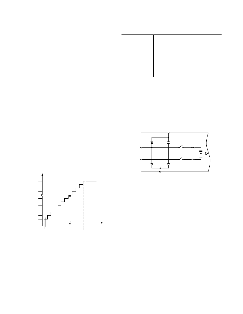
Analog Inputs
Figure 4 shows a simplified analog input section of the AD7654.
INAx
INBx
AGND
AVDD
C
S
C
S
R
B
= 500
R
A
= 500
Figure 4. Simplified Analog Input
The diodes shown in Figure 4 provide ESD protection for the
inputs. Care must be taken to ensure that the analog input
signal never exceeds the absolute ratings on these inputs. This
will cause these diodes to become forward-biased and start
conducting current. These diodes can handle a forward-biased
current of 120 mA maximum. This condition could eventually
occur when the input buffer’s (U1) or (U2) supplies are different
from AVDD. In such case, an input buffer with a short-circuit
current limitation can be used to protect the part.
This analog input structure allows the sampling of the differential
signal between INx and INxN. Unlike other converters, the
INxN is sampled at the same time as the INx input. By using
these differential inputs, small signals common to both inputs
are rejected.
相關PDF資料 |
PDF描述 |
|---|---|
| AD7654ASTRL | Dual 2-Channel Simultaneous Sampling SAR 500 kSPS 16-Bit ADC |
| AD7655 | Low Cost 4-Channel 1 MSPS 16-Bit ADC |
| AD7655ACP | Low Cost 4-Channel 1 MSPS 16-Bit ADC |
| AD7655ACPRL | Low Cost 4-Channel 1 MSPS 16-Bit ADC |
| AD7655AST | Low Cost 4-Channel 1 MSPS 16-Bit ADC |
相關代理商/技術參數 |
參數描述 |
|---|---|
| AD7654ASTRL | 制造商:Analog Devices 功能描述:ADC Single SAR 500ksps 16-bit Parallel/Serial 48-Pin LQFP T/R |
| AD7654ASTZ | 功能描述:IC ADC 16BIT 500KSPS DUAL 48LQFP RoHS:是 類別:集成電路 (IC) >> 數據采集 - 模數轉換器 系列:PulSAR® 標準包裝:1 系列:microPOWER™ 位數:8 采樣率(每秒):1M 數據接口:串行,SPI? 轉換器數目:1 功率耗散(最大):- 電壓電源:模擬和數字 工作溫度:-40°C ~ 125°C 安裝類型:表面貼裝 封裝/外殼:24-VFQFN 裸露焊盤 供應商設備封裝:24-VQFN 裸露焊盤(4x4) 包裝:Digi-Reel® 輸入數目和類型:8 個單端,單極 產品目錄頁面:892 (CN2011-ZH PDF) 其它名稱:296-25851-6 |
| AD7654ASTZ | 制造商:Analog Devices 功能描述:IC 16BIT ADC SMD 7654 LQFP48 |
| AD7654ASTZRL | 功能描述:IC ADC 16BIT DUAL 2CH 48LQFP RoHS:是 類別:集成電路 (IC) >> 數據采集 - 模數轉換器 系列:PulSAR® 標準包裝:1,000 系列:- 位數:12 采樣率(每秒):300k 數據接口:并聯 轉換器數目:1 功率耗散(最大):75mW 電壓電源:單電源 工作溫度:0°C ~ 70°C 安裝類型:表面貼裝 封裝/外殼:24-SOIC(0.295",7.50mm 寬) 供應商設備封裝:24-SOIC 包裝:帶卷 (TR) 輸入數目和類型:1 個單端,單極;1 個單端,雙極 |
| AD7655 | 制造商:AD 制造商全稱:Analog Devices 功能描述:14-Bit, 1 MSPS, Differential, Programmable Input PulSAR ADC |
發布緊急采購,3分鐘左右您將得到回復。