- 您現(xiàn)在的位置:買賣IC網(wǎng) > PDF目錄373913 > AD7703CR (ANALOG DEVICES INC) ECONOLINE: REC2.2-S_DRW(Z)/H* - 2.2W DIP Package- 1kVDC Isolation- Regulated Output- 4.5-9V, 9-18V, 18-36V, 36-72V Wide Input Range 2 : 1- UL94V-0 Package Material- Continuous Short Circiut Protection- Cost Effective- 100% Burned In- Efficiency to 84% PDF資料下載
參數(shù)資料
| 型號: | AD7703CR |
| 廠商: | ANALOG DEVICES INC |
| 元件分類: | ADC |
| 英文描述: | ECONOLINE: REC2.2-S_DRW(Z)/H* - 2.2W DIP Package- 1kVDC Isolation- Regulated Output- 4.5-9V, 9-18V, 18-36V, 36-72V Wide Input Range 2 : 1- UL94V-0 Package Material- Continuous Short Circiut Protection- Cost Effective- 100% Burned In- Efficiency to 84% |
| 中文描述: | 1-CH 20-BIT DELTA-SIGMA ADC, SERIAL ACCESS, PDSO20 |
| 封裝: | MS-013AC, SOIC-20 |
| 文件頁數(shù): | 4/16頁 |
| 文件大小: | 251K |
| 代理商: | AD7703CR |
AD7703
–4–
REV. D
(AV
DD
= DV
DD
= +5 V
6
10%; AV
SS
= DV
SS
= –5 V
6
10%; AGND = DGND = 0 V; f
CLKIN
=
4.096 MHz; Input Levels: Logic 0 = 0 V, Logic 1 = DV
DD
; unless otherwse noted.)
Limit at T
MIN
, T
MAX
(S Version)
Units
Conditions/Comment
6
TIMNGCHARACTERISTICS
1, 2
Limit at T
MIN
, T
MAX
(A, B, C Versions)
Parameter
f
CLK IN3, 4
200
5
200
5
50
50
0
50
1000
200
5
200
5
50
50
0
50
1000
kHz min
MHz max
kHz min
MHz max
ns max
ns max
ns min
ns min
ns min
Master Clock Frequency: Internal Gate Oscillator
T ypically 4096 kHz
Master Clock Frequency: Externally Supplied
t
r5
t
f5
t
1
t
2
t
36
Digital Output Rise T ime. T ypically 20 ns
Digital Output Fall T ime. T ypically 20 ns
SC1, SC2 to CAL High Setup T ime
SC1, SC2 Hold T ime After CAL Goes High
SLEEP
High to CLK IN High Setup T ime
SSC MODE
t
47
t
5
t
6
t
7
t
8
t
t
9
3/f
CLK IN
100
250
300
790
l/f
CLK IN
+ 200
4/f
CLK IN
+ 200
3/f
CLK IN
100
250
300
790
l/f
CLK IN
+ 200
4/f
CLK IN
+ 200
ns max
ns max
ns min
ns max
ns max
ns max
ns max
Data Access T ime (
CS
Low to Data Valid)
SCLK Falling Edge to Data Valid Delay (25 ns typ)
MSB Data Setup T ime. T ypically 380 ns
SCLK High Pulse Width. T ypically 240 ns
SCLK Low Pulse Width. T ypically 730 ns
SCLK Rising Edge to Hi-Z Delay (1/f
CLK IN
+ 100 ns typ)
CS
High to Hi-Z Delay
SEC MODE
f
SCLK
t
11
t
12
t
137, 10
t
1411
t
158
t
168
5
35
160
160
150
250
200
5
35
160
160
150
250
200
MHz max
ns min
ns min
ns max
ns max
ns max
ns max
Serial Clock Input Frequency
SCLK High Pulse Width
SCLK Low Pulse Width
Data Access T ime (
CS
Low to Data Valid). T ypically 80 ns
SCLK Falling Edge to Data Valid Delay. T ypically 75 ns
CS
High to Hi-Z Delay
SCLK Falling Edge to Hi-Z Delay. T ypically 100 ns
NOT ES
Sample tested at +25
°
C to ensure compliance. All input signals are specified with tr = tf = 5 ns (10% to 90% of 5 V) and timed from a voltage level of 1.6 V.
2
See Figures 1 to 6.
3
CLK IN duty cycle range is 20% to 80%. CLK IN must be supplied whenever the AD7703 is not in SLEEP mode. If no clock is present in this case, the device can
draw higher current than specified and possibly become uncalibrated.
4
T he AD7703 is production tested with f
CLK IN
at 4.096 MHz. It is guaranteed by characterization to operate at 200 kHz.
5
Specified using 10% and 90% points on waveform of interest.
6
In order to synchronize several AD7703s together using the
SLEEP
pin, this specification must be met.
7
t
4
and t
13
are measured with the load circuit of Figure 1 and defined as the time required for an output to cross 0.8 V or 2.4 V.
8
t
9
, t
10
, t
15
and t
16
are derived from the measured time taken by the data outputs to change 0.5 V when loaded with the circuit of Figure 1. T he measured number is
then extrapolated back to remove the effects of charging or discharging the 100 pF capacitor. T his means that the tune quoted in the T iming Characteristics is the
true bus relinquish time of the part and as such is independent of external bus loading capacitances.
9
If
CS
is returned high before all 20 bits are output, the SDAT A and SCLK outputs will complete the current data bit and then go to high impedance.
10
If
CS
is activated asynchronously to
DRDY
,
CS
will not be recognized if it occurs when
DRDY
is high for four clock cycles. T he propagation delay time may be as
great as 4 CLK IN cycles plus 160 ns. T o guarantee proper clocking of SDAT A when using asynchronous
CS
, the SCLK input should not be taken high sooner than
4 CLK IN cycles plus 160 ns after
CS
goes low.
11
SDAT A is clocked out on the falling edge of the SCLK input.
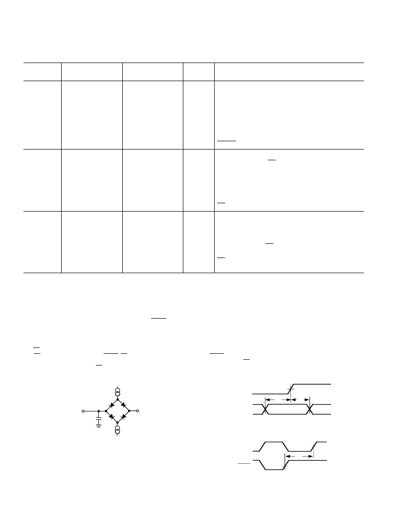
CAL
SC1, SC2
SC1,SC2 VALID
t
1
t
2
Figure 2. Calibration Control Timing
CLKIN
SLEEP
t
3
Figure 3. Sleep Mode Timing
I
1.6mA
+2.1V
TO
OUTPUT
PIN
C
L
100pF
I
200μA
Figure 1. Load Circuit for Access Time and Bus Relinquish
Time
相關(guān)PDF資料 |
PDF描述 |
|---|---|
| AD7703SQ | LC2MOS 20-Bit A/D Converter |
| AD7705 | 3 V/5 V, 1 mW 2-/3-Channel 16-Bit, Sigma-Delta ADCs |
| AD7705BN | ECONOLINE: REC2.2-S_DR/H1 - 2.2W DIP Package- 1kVDC Isolation- Regulated Output- UL94V-0 Package Material- Continuous Short Circiut Protection- Internal SMD design- 100% Burned In- Efficiency to 75% |
| AD7705BR | ECONOLINE: REC2.2-S_DRW(Z)/H* - 2.2W DIP Package- 1kVDC Isolation- Regulated Output- 4.5-9V, 9-18V, 18-36V, 36-72V Wide Input Range 2 : 1- UL94V-0 Package Material- Continuous Short Circiut Protection- Cost Effective- 100% Burned In- Efficiency to 84% |
| AD7705BRU | 3 V/5 V, 1 mW 2-/3-Channel 16-Bit, Sigma-Delta ADCs |
相關(guān)代理商/技術(shù)參數(shù) |
參數(shù)描述 |
|---|---|
| AD7703CR-REEL | 功能描述:IC ADC 20BIT LC2MOS MONO 20-SOIC RoHS:否 類別:集成電路 (IC) >> 數(shù)據(jù)采集 - 模數(shù)轉(zhuǎn)換器 系列:- 標(biāo)準(zhǔn)包裝:1 系列:- 位數(shù):14 采樣率(每秒):83k 數(shù)據(jù)接口:串行,并聯(lián) 轉(zhuǎn)換器數(shù)目:1 功率耗散(最大):95mW 電壓電源:雙 ± 工作溫度:0°C ~ 70°C 安裝類型:通孔 封裝/外殼:28-DIP(0.600",15.24mm) 供應(yīng)商設(shè)備封裝:28-PDIP 包裝:管件 輸入數(shù)目和類型:1 個單端,雙極 |
| AD7703CRZ | 功能描述:IC ADC 20BIT LC2MOS MONO 20SOIC RoHS:是 類別:集成電路 (IC) >> 數(shù)據(jù)采集 - 模數(shù)轉(zhuǎn)換器 系列:- 標(biāo)準(zhǔn)包裝:1 系列:- 位數(shù):14 采樣率(每秒):83k 數(shù)據(jù)接口:串行,并聯(lián) 轉(zhuǎn)換器數(shù)目:1 功率耗散(最大):95mW 電壓電源:雙 ± 工作溫度:0°C ~ 70°C 安裝類型:通孔 封裝/外殼:28-DIP(0.600",15.24mm) 供應(yīng)商設(shè)備封裝:28-PDIP 包裝:管件 輸入數(shù)目和類型:1 個單端,雙極 |
| AD7703SQ | 制造商:AD 制造商全稱:Analog Devices 功能描述:LC2MOS 20-Bit A/D Converter |
| AD7705 | 制造商:AD 制造商全稱:Analog Devices 功能描述:3 V/5 V, 1 mW 2-/3-Channel 16-Bit, Sigma-Delta ADCs |
| AD7705_06 | 制造商:AD 制造商全稱:Analog Devices 功能描述:3 V/5 V, 1 mW, 2-/3-Channel, 16-Bit, Sigma-Delta ADCs |
發(fā)布緊急采購,3分鐘左右您將得到回復(fù)。