- 您現(xiàn)在的位置:買賣IC網(wǎng) > PDF目錄373913 > AD7703CR (ANALOG DEVICES INC) ECONOLINE: REC2.2-S_DRW(Z)/H* - 2.2W DIP Package- 1kVDC Isolation- Regulated Output- 4.5-9V, 9-18V, 18-36V, 36-72V Wide Input Range 2 : 1- UL94V-0 Package Material- Continuous Short Circiut Protection- Cost Effective- 100% Burned In- Efficiency to 84% PDF資料下載
參數(shù)資料
| 型號(hào): | AD7703CR |
| 廠商: | ANALOG DEVICES INC |
| 元件分類: | ADC |
| 英文描述: | ECONOLINE: REC2.2-S_DRW(Z)/H* - 2.2W DIP Package- 1kVDC Isolation- Regulated Output- 4.5-9V, 9-18V, 18-36V, 36-72V Wide Input Range 2 : 1- UL94V-0 Package Material- Continuous Short Circiut Protection- Cost Effective- 100% Burned In- Efficiency to 84% |
| 中文描述: | 1-CH 20-BIT DELTA-SIGMA ADC, SERIAL ACCESS, PDSO20 |
| 封裝: | MS-013AC, SOIC-20 |
| 文件頁(yè)數(shù): | 6/16頁(yè) |
| 文件大小: | 251K |
| 代理商: | AD7703CR |
第1頁(yè)第2頁(yè)第3頁(yè)第4頁(yè)第5頁(yè)當(dāng)前第6頁(yè)第7頁(yè)第8頁(yè)第9頁(yè)第10頁(yè)第11頁(yè)第12頁(yè)第13頁(yè)第14頁(yè)第15頁(yè)第16頁(yè)
AD7703
–6–
REV. D
PIN FUNCT ION DE SCRIPT ION
Pin
Mnemonic
Description
1
MODE
Selects the Serial Interface Mode. If MODE is tied to DGND, the Synchronous External Clocking (SEC)
mode is selected. SCLK is configured as an input, and the output appears without formatting, the MSB com-
ing first. If MODE is tied to +5 V, the AD7703 operates in the Synchronous Self-Clocking (SSC) mode.
SCLK is configured as an output, with a clock frequency for f
CLK IN
/4 and 25% duty cycle.
Clock Output to generate an Internal Master Clock by connecting a crystal between CLK OUT and CLK IN.
If an external clock is used, CLK OUT is not connected.
Clock Input for External Clock.
System Calibration Pins. T he state of these pins, when CAL is taken high, determines the type of calibration
performed.
Digital Ground. Ground reference for all digital signals.
Digital Negative Supply, –5 V nominal.
Analog Negative Supply, –5 V nominal.
Analog Ground. Ground reference for all analog signals.
Analog Input.
Voltage Reference Input, +2.5 V nominal. T his determines the value of positive full-scale in the unipolar
mode and of both positive and negative full-scale in the Bipolar Mode.
Sleep mode pin. When this pin is taken low, the AD7703 goes into a low-power mode with typically 10
μ
W
power consumption.
Bipolar/Unipolar mode pin. When this pin is Low, the AD7703 is configured for a unipolar input range going
from AGND to V
REF
. When Pin 12 is High, the AD7703 is configured for a bipolar input range,
±
V
REF
.
Calibration mode pin. When CAL is taken High for more than 4 cycles, the AD7703 is reset and performs a
calibration cycle when CAL is brought Low again. T he CAL pin can also be used as a strobe to synchronize
the operation of several AD7703s.
Analog Positive Supply, +5 V nominal.
Digital Positive Supply, +5 V nominal.
Chip Select Input. When
CS
is brought low, the AD7703 will begin to transmit serial data in a format deter-
mined by the state of the MODE pin.
Data Ready Output.
DRDY
is low when valid data is available in the output register. It goes high after trans-
mission of a word is completed. It also goes high for four clock cycles when a new data word is being loaded
into the output register, to indicate that valid data is not available, irrespective of whether data transmission is
complete or not.
Serial Clock Input/Output. T he SCLK pin in configured as an input or output, dependent on the type of se-
rial data transmission that has been selected by the MODE pin. When configured as an output in the Syn-
chronous Self-Clocking mode, it has a frequency of f
CLK IN
/4 and a duty cycle of 25%.
Serial Data Output. T he AD7703’s output data is available at this pin as a 20-bit serial word.
2
CLK OUT
3
4, 17
CLK IN
SC1, SC2
5
6
7
8
9
10
DGND
DV
SS
AV
SS
AGND
A
IN
V
REF
11
SLEEP
12
BP/
UP
13
CAL
14
15
16
AV
DD
DV
DD
CS
18
DRDY
19
SCLK
20
SDAT A
T able I. Bit Weight T able (2.5 V Reference Voltage)
UNIPOLAR MODE
LSBs
% FS
BIPOLAR MODE
ppm FS LSBs
m
V
% FS
ppm FS
0.596
1.192
2.384
4.768
9.537
0.25
0.5
1.00
2.00
4.00
0.0000238
0.0000477
0.0000954
0.0001907
0.0003814
0.24
0.48
0.95
1.91
3.81
0.13
0.26
0.5
1.00
2.00
0.0000119
0.0000238
0.0000477
0.0000954
0.0001907
0.12
0.24
0.48
0.95
1.91
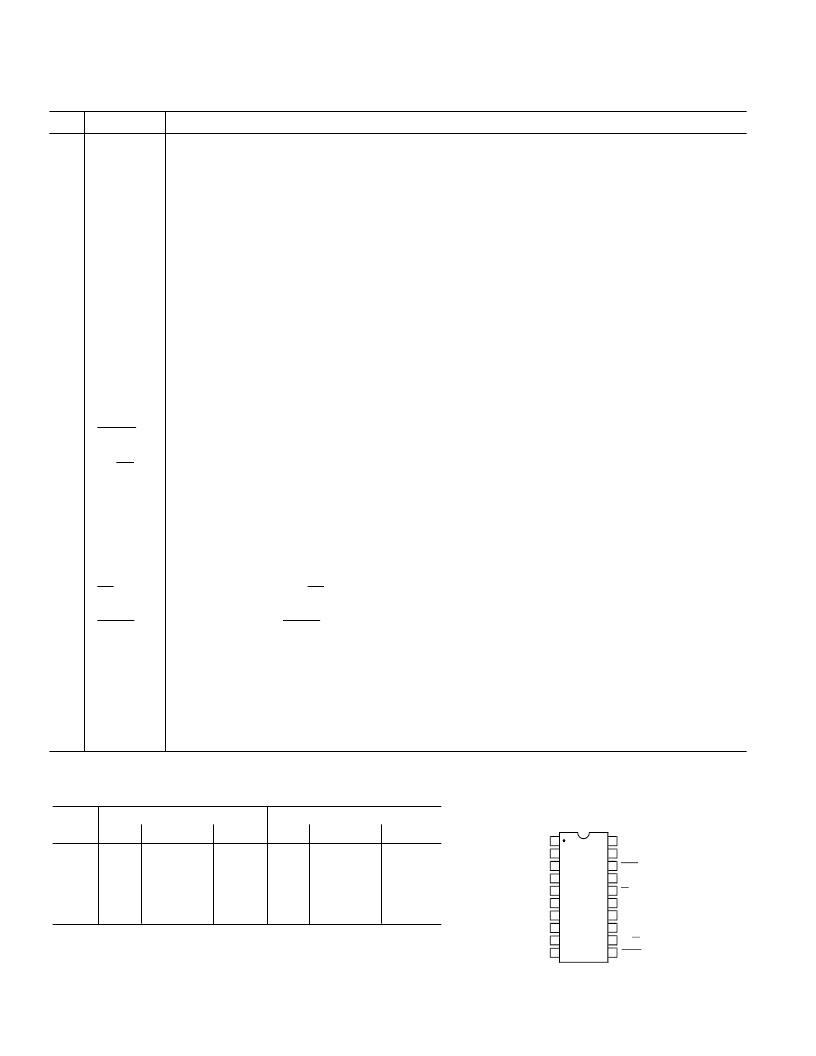
PIN CONFIGURAT ION
DIP, Cerdip, SOIC
MODE
SC1
DGND
DV
SS
AV
SS
CLKOUT
CLKIN
AGND
A
IN
V
REF
SDATA
SCLK
SC2
CAL
AV
DD
DV
DD
DRDY
CS
BP/UP
SLEEP
TOP VIEW
(Not to Scale)
AD7703
1
2
3
4
5
6
7
8
9
10
14
13
12
11
20
19
18
17
16
15
相關(guān)PDF資料 |
PDF描述 |
|---|---|
| AD7703SQ | LC2MOS 20-Bit A/D Converter |
| AD7705 | 3 V/5 V, 1 mW 2-/3-Channel 16-Bit, Sigma-Delta ADCs |
| AD7705BN | ECONOLINE: REC2.2-S_DR/H1 - 2.2W DIP Package- 1kVDC Isolation- Regulated Output- UL94V-0 Package Material- Continuous Short Circiut Protection- Internal SMD design- 100% Burned In- Efficiency to 75% |
| AD7705BR | ECONOLINE: REC2.2-S_DRW(Z)/H* - 2.2W DIP Package- 1kVDC Isolation- Regulated Output- 4.5-9V, 9-18V, 18-36V, 36-72V Wide Input Range 2 : 1- UL94V-0 Package Material- Continuous Short Circiut Protection- Cost Effective- 100% Burned In- Efficiency to 84% |
| AD7705BRU | 3 V/5 V, 1 mW 2-/3-Channel 16-Bit, Sigma-Delta ADCs |
相關(guān)代理商/技術(shù)參數(shù) |
參數(shù)描述 |
|---|---|
| AD7703CR-REEL | 功能描述:IC ADC 20BIT LC2MOS MONO 20-SOIC RoHS:否 類別:集成電路 (IC) >> 數(shù)據(jù)采集 - 模數(shù)轉(zhuǎn)換器 系列:- 標(biāo)準(zhǔn)包裝:1 系列:- 位數(shù):14 采樣率(每秒):83k 數(shù)據(jù)接口:串行,并聯(lián) 轉(zhuǎn)換器數(shù)目:1 功率耗散(最大):95mW 電壓電源:雙 ± 工作溫度:0°C ~ 70°C 安裝類型:通孔 封裝/外殼:28-DIP(0.600",15.24mm) 供應(yīng)商設(shè)備封裝:28-PDIP 包裝:管件 輸入數(shù)目和類型:1 個(gè)單端,雙極 |
| AD7703CRZ | 功能描述:IC ADC 20BIT LC2MOS MONO 20SOIC RoHS:是 類別:集成電路 (IC) >> 數(shù)據(jù)采集 - 模數(shù)轉(zhuǎn)換器 系列:- 標(biāo)準(zhǔn)包裝:1 系列:- 位數(shù):14 采樣率(每秒):83k 數(shù)據(jù)接口:串行,并聯(lián) 轉(zhuǎn)換器數(shù)目:1 功率耗散(最大):95mW 電壓電源:雙 ± 工作溫度:0°C ~ 70°C 安裝類型:通孔 封裝/外殼:28-DIP(0.600",15.24mm) 供應(yīng)商設(shè)備封裝:28-PDIP 包裝:管件 輸入數(shù)目和類型:1 個(gè)單端,雙極 |
| AD7703SQ | 制造商:AD 制造商全稱:Analog Devices 功能描述:LC2MOS 20-Bit A/D Converter |
| AD7705 | 制造商:AD 制造商全稱:Analog Devices 功能描述:3 V/5 V, 1 mW 2-/3-Channel 16-Bit, Sigma-Delta ADCs |
| AD7705_06 | 制造商:AD 制造商全稱:Analog Devices 功能描述:3 V/5 V, 1 mW, 2-/3-Channel, 16-Bit, Sigma-Delta ADCs |
發(fā)布緊急采購(gòu),3分鐘左右您將得到回復(fù)。