- 您現在的位置:買賣IC網 > PDF目錄373913 > AD7705BRU (ANALOG DEVICES INC) 3 V/5 V, 1 mW 2-/3-Channel 16-Bit, Sigma-Delta ADCs PDF資料下載
參數資料
| 型號: | AD7705BRU |
| 廠商: | ANALOG DEVICES INC |
| 元件分類: | ADC |
| 英文描述: | 3 V/5 V, 1 mW 2-/3-Channel 16-Bit, Sigma-Delta ADCs |
| 中文描述: | 2-CH 16-BIT DELTA-SIGMA ADC, SERIAL ACCESS, PDSO16 |
| 封裝: | MO-153AB, TSSOP-16 |
| 文件頁數: | 3/32頁 |
| 文件大小: | 264K |
| 代理商: | AD7705BRU |
第1頁第2頁當前第3頁第4頁第5頁第6頁第7頁第8頁第9頁第10頁第11頁第12頁第13頁第14頁第15頁第16頁第17頁第18頁第19頁第20頁第21頁第22頁第23頁第24頁第25頁第26頁第27頁第28頁第29頁第30頁第31頁第32頁
–3–
REV. A
AD7705/AD7706
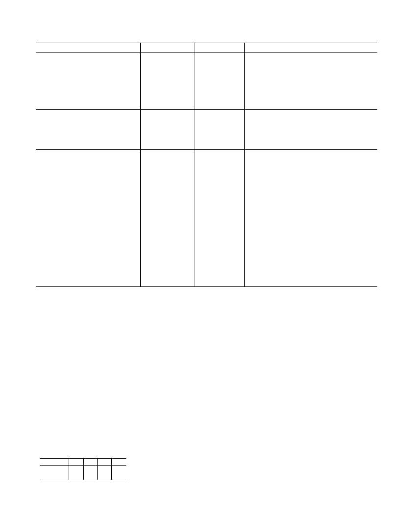
Parameter
B Version
1
Units
Conditions/Comments
LOGIC OUTPUTS (Including MCLK OUT)
V
OL
, Output Low Voltage
V
OL
, Output Low Voltage
V
OH
, Output High Voltage
V
, Output High Voltage
Floating State Leakage Current
Floating State Output Capacitance
13
Data Output Coding
0.4
0.4
4
V
–0.6
±
10
9
Binary
Offset Binary
V max
V max
V min
V min
μ
A max
pF typ
I
SINK
= 800
μ
A Except for MCLK OUT.
12
V
DD
= 5 V.
I
SINK
= 100
μ
A Except for MCLK OUT.
12
V
DD
= 3 V.
I
SOURCE
= 200
μ
A Except for MCLK OUT.
12
DD
= 5 V.
I
SOURCE
= 100
μ
A Except for MCLK OUT.
12
V
DD
= 3 V.
Unipolar Mode
Bipolar Mode
SYSTEM CALIBRATION
Positive Full-Scale Calibration Limit
14
Negative Full-Scale Calibration Limit
14
Offset Calibration Limit
14
Input Span
(1.05
×
V
REF
)/GAIN
–(1.05
×
V
REF
)/GAIN
–(1.05
×
V
REF
)/GAIN
(0.8
×
V
REF
(2.1
×
V
REF
)/GAIN
V max
V max
V max
V min
V max
GAIN Is the Selected PGA Gain (1 to 128)
GAIN Is the Selected PGA Gain (1 to 128)
GAIN Is the Selected PGA Gain (1 to 128)
GAIN Is the Selected PGA Gain (1 to 128)
GAIN Is the Selected PGA Gain (1 to 128)
POWER REQUIREMENTS
V
DD
Voltage
Power Supply Currents
16
+2.7 to +3.3
V min to V max
For Specified Performance
Digital I/Ps = 0V or V
DD
. External MCLK IN and
CLK DIS = 1
BUF Bit = 0. f
CLKIN
= 1MHz. Gains of 1 to 128
BUF Bit = 1. f
CLKIN
= 1MHz. Gains of 1 to 128
BUF Bit = 0. f
CLKIN
= 2.4576MHz. Gains of 1 to 4
BUF Bit = 0. f
CLKIN
= 2.4576MHz. Gains of 8 to 128
BUF Bit = 1. f
CLKIN
= 2.4576MHz. Gains of 1 to 4
BUF Bit = 1. f
CLKIN
= 2.4576MHz. Gains of 8 to 128
For Specified Performance
Digital I/Ps = 0V or V
DD
. External MCLK IN and
CLK DIS = 1.
BUF Bit = 0. f
CLKIN
= 1MHz. Gains of 1 to 128
BUF Bit = 1. f
CLKIN
= 1MHz. Gains of 1 to 128
BUF Bit = 0. f
CLKIN
= 2.4576MHz. Gains of 1 to 4
BUF Bit = 0. f
CLKIN
= 2.4576MHz. Gains of 8 to 128
BUF Bit = 1. f
CLKIN
= 2.4576MHz. Gains of 1 to 4
BUF Bit = 1. f
CLKIN
= 2.4576MHz. Gains of 8 to 128
External MCLK IN = 0 V or V
DD
. V
DD
= 5 V. See Figure 9
External MCLK IN = 0 V or V
DD
. V
DD
= 3 V
0.32
0.6
0.4
0.6
0.7
1.1
+4.75 to +5.25
mA max
mA max
mA max
mA max
mA max
mA max
V min to V max
V
DD
Voltage
Power Supply Currents
16
0.45
0.7
0.6
0.85
0.9
1.3
16
8
See Note 19
mA max
mA max
mA max
mA max
mA max
mA max
μ
A max
μ
A max
dB typ
Standby (Power-Down) Current
17
Power Supply Rejection
18
NOTES
Temperature range as follows: B Version, –40
°
C to +85
°
C.
2
These numbers are established from characterization or design at initial product release.
3
A calibration is effectively a conversion so these errors will be of the order of the conversion noise shown in Tables I and III. This applies after calibration at the
temperature of interest.
4
Recalibration at any temperature will remove these drift errors.
5
Positive Full-Scale Error includes Zero-Scale Errors (Unipolar Offset Error or Bipolar Zero Error) and applies to both unipolar and bipolar input ranges.
6
Full-Scale Drift includes Zero-Scale Drift (Unipolar Offset Drift or Bipolar Zero Drift) and applies to both unipolar and bipolar input ranges.
7
Gain Error does not include Zero-Scale Errors. It is calculated as Full-Scale Error–Unipolar Offset Error for unipolar ranges and Full-Scale Error–Bipolar Zero Error for
bipolar ranges.
8
Gain Error Drift does not include Unipolar Offset Drift/Bipolar Zero Drift. It is effectively the drift of the part if zero scale calibrations only were performed.
9
This common-mode voltage range is allowed provided that the input voltage on analog inputs does not go more positive than V
DD
+ 30 mV or go more negative than
GND – 30mV. Parts are functional with voltages down to GND – 200 mV, but with increased leakage at high temperature.
10
The analog input voltage range on AIN(+) is given here with respect to the voltage on AIN(–) on the AD7705 and is given with respect to the COMMON input on the
AD7706. The absolute voltage on the analog inputs should not go more positive than V
DD
+ 30mV, or go more negative than GND– 30mV for specified performance, input
voltages of GND – 200 mV can be accommodated, but with increased leakage at high temperature.
11
V
REF
= REF IN(+) – REF IN(–).
12
These logic output levels apply to the MCLK OUT only when it is loaded with one CMOS load.
13
Sample tested at +25
°
C to ensure compliance.
14
After calibration, if the analog input exceeds positive full scale, the converter will output all 1s. If the analog input is less than negative full scale, the device will output all 0s.
15
These calibration and span limits apply provided the absolute voltage on the analog inputs does not exceed V
DD
+ 30mV or go more negative than GND – 30mV. The offset
calibration limit applies to both the unipolar zero point and the bipolar zero point.
16
When using a crystal or ceramic resonator across the MCLK pins as the clock source for the device, the V
DD
current and power dissipation will vary depending on the crystal or
resonator type (see Clocking and Oscillator Circuit section).
17
If the external master clock continues to run in standby mode, the standby current increases to 150
μ
A typical at 5 V and 75
μ
A at 3 V. When using a crystal or ceramic
resonator across the MCLK pins as the clock source for the device, the internal oscillator continues to run in standby mode and the power dissipation depends on the crystal
or resonator type (see Standby Mode section).
18
Measured at dc and applies in the selected passband. PSRR at 50Hz will exceed 120dB with filter notches of 25 Hz or 50Hz. PSRR at 60Hz will exceed 120dB with filter
notches of 20 Hz or 60Hz.
19
PS
RR depends on both gain and V
DD
.
Gain
V
DD
= 3 V
V
DD
= 5 V
1
86
90
2
78
78
4
85
84
8–128
93
91
Specifications subject to change without notice.
相關PDF資料 |
PDF描述 |
|---|---|
| AD7706 | 3 V/5 V, 1 mW 2-/3-Channel 16-Bit, Sigma-Delta ADCs |
| AD7706BN | ECONOLINE: REC2.2-S_DRW(Z)/H* - 2.2W DIP Package- 1kVDC Isolation- Regulated Output- 4.5-9V, 9-18V, 18-36V, 36-72V Wide Input Range 2 : 1- UL94V-0 Package Material- Continuous Short Circiut Protection- Cost Effective- 100% Burned In- Efficiency to 84% |
| AD7706BR | 3 V/5 V, 1 mW 2-/3-Channel 16-Bit, Sigma-Delta ADCs |
| AD7706BRU | 3 V/5 V, 1 mW 2-/3-Channel 16-Bit, Sigma-Delta ADCs |
| AD7705EB | Precision Zero-Drift Operational Amplifier with Internal Capacitors; Package: SO; No of Pins: 8; Temperature Range: 0°C to +70°C |
相關代理商/技術參數 |
參數描述 |
|---|---|
| AD7705BRU-REEL | 功能描述:IC ADC 16BIT 2CH 16-TSSOP T/R RoHS:否 類別:集成電路 (IC) >> 數據采集 - 模數轉換器 系列:- 標準包裝:1,000 系列:- 位數:16 采樣率(每秒):45k 數據接口:串行 轉換器數目:2 功率耗散(最大):315mW 電壓電源:模擬和數字 工作溫度:0°C ~ 70°C 安裝類型:表面貼裝 封裝/外殼:28-SOIC(0.295",7.50mm 寬) 供應商設備封裝:28-SOIC W 包裝:帶卷 (TR) 輸入數目和類型:2 個單端,單極 |
| AD7705BRU-REEL7 | 功能描述:IC ADC 16BIT 2CH 16-TSSOP T/R RoHS:否 類別:集成電路 (IC) >> 數據采集 - 模數轉換器 系列:- 標準包裝:1,000 系列:- 位數:16 采樣率(每秒):45k 數據接口:串行 轉換器數目:2 功率耗散(最大):315mW 電壓電源:模擬和數字 工作溫度:0°C ~ 70°C 安裝類型:表面貼裝 封裝/外殼:28-SOIC(0.295",7.50mm 寬) 供應商設備封裝:28-SOIC W 包裝:帶卷 (TR) 輸入數目和類型:2 個單端,單極 |
| AD7705BRUZ | 功能描述:IC ADC 16BIT 2CH 16-TSSOP RoHS:是 類別:集成電路 (IC) >> 數據采集 - 模數轉換器 系列:- 標準包裝:1 系列:microPOWER™ 位數:8 采樣率(每秒):1M 數據接口:串行,SPI? 轉換器數目:1 功率耗散(最大):- 電壓電源:模擬和數字 工作溫度:-40°C ~ 125°C 安裝類型:表面貼裝 封裝/外殼:24-VFQFN 裸露焊盤 供應商設備封裝:24-VQFN 裸露焊盤(4x4) 包裝:Digi-Reel® 輸入數目和類型:8 個單端,單極 產品目錄頁面:892 (CN2011-ZH PDF) 其它名稱:296-25851-6 |
| AD7705BRUZ | 制造商:Analog Devices 功能描述:IC 制造商:Analog Devices 功能描述:IC, ADC, 16BIT, 500SPS, TSSOP-16 |
| AD7705BRUZ | 制造商:Analog Devices 功能描述:ADC 2CH 16BIT SIG DEL 16TSSOP |
發布緊急采購,3分鐘左右您將得到回復。