- 您現在的位置:買賣IC網 > PDF目錄373913 > AD7705BRU (ANALOG DEVICES INC) 3 V/5 V, 1 mW 2-/3-Channel 16-Bit, Sigma-Delta ADCs PDF資料下載
參數資料
| 型號: | AD7705BRU |
| 廠商: | ANALOG DEVICES INC |
| 元件分類: | ADC |
| 英文描述: | 3 V/5 V, 1 mW 2-/3-Channel 16-Bit, Sigma-Delta ADCs |
| 中文描述: | 2-CH 16-BIT DELTA-SIGMA ADC, SERIAL ACCESS, PDSO16 |
| 封裝: | MO-153AB, TSSOP-16 |
| 文件頁數: | 7/32頁 |
| 文件大小: | 264K |
| 代理商: | AD7705BRU |
第1頁第2頁第3頁第4頁第5頁第6頁當前第7頁第8頁第9頁第10頁第11頁第12頁第13頁第14頁第15頁第16頁第17頁第18頁第19頁第20頁第21頁第22頁第23頁第24頁第25頁第26頁第27頁第28頁第29頁第30頁第31頁第32頁
AD7705/AD7706
–7–
REV. A
Pin No.
Mnemonic
Function
10
REF IN(–)
Reference Input. Negative input of the differential reference input to the AD7705/AD7706.
The REFIN(–) can lie anywhere between V
DD
and GND provided REFIN(+) is greater
than REFIN(–).
AD7705: Negative input of the differential analog Input Channel 2. AD7706: Analog Input
Channel 3.
Logic Output. A logic low on this output indicates that a new output word is available from
the AD7705/AD7706 data register. The
DRDY
pin will return high upon completion of a
read operation of a full output word. If no data read has taken place between output updates,
the
DRDY
line will return high for 500
×
t
CLKIN
cycles prior to the next output update.
While
DRDY
is high, a read operation should neither be attempted nor in progress to avoid
reading from the data register as it is being updated. The
DRDY
line will return low again
when the update has taken place.
DRDY
is also used to indicate when the AD7705/AD7706
has completed its on-chip calibration sequence.
Serial Data Output with serial data being read from the output shift register on the part. This
output shift register can contain information from the setup register, communications regis-
ter, clock register or data register, depending on the register selection bits of the Communica-
tions Register.
Serial Data Input with serial data being written to the input shift register on the part. Data
from this input shift register is transferred to the setup register, clock register or communica-
tions register, depending, on the register selection bits of the Communications Register.
Supply Voltage, +2.7 V to +5.25 V operation.
Ground reference point for the AD7705/AD7706’s internal circuitry.
11
AIN2(–)[AIN3]
12
DRDY
13
DOUT
14
DIN
15
16
V
DD
GND
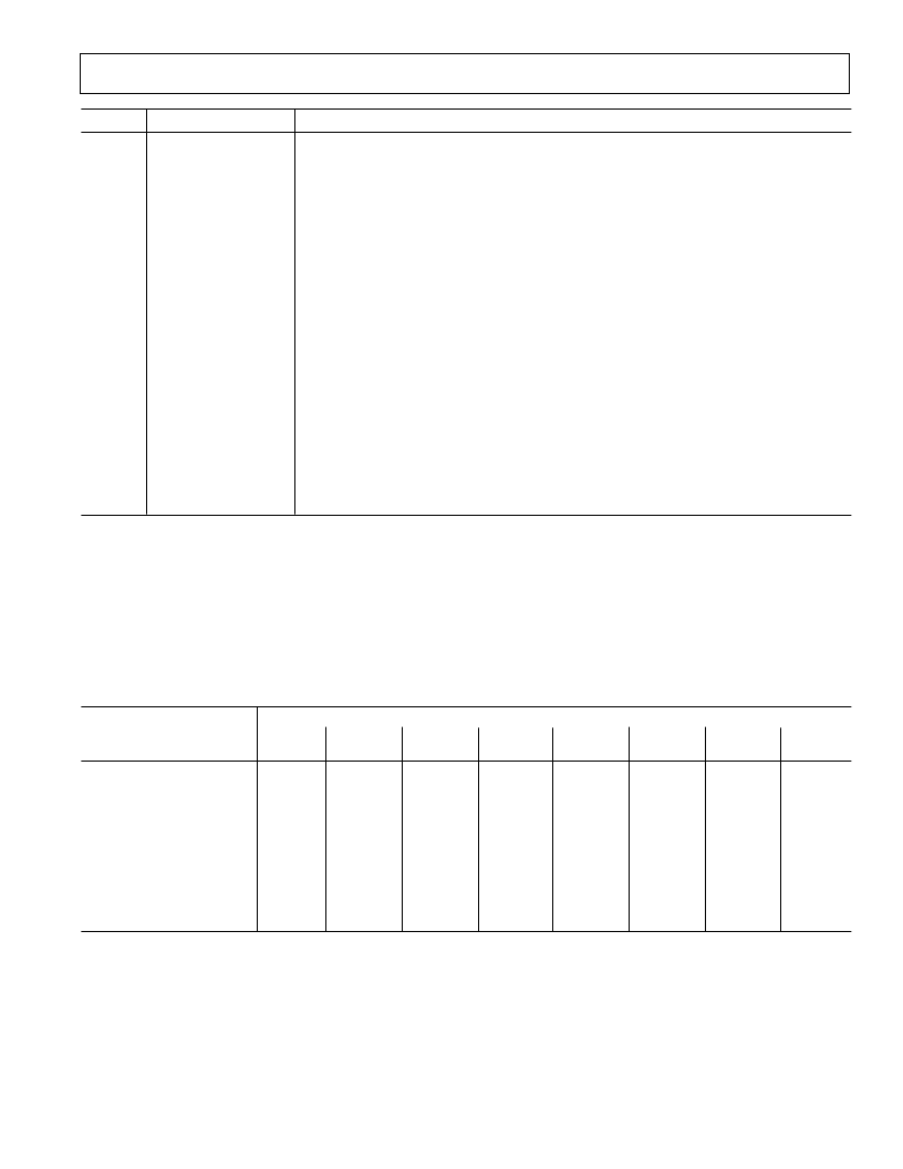
OUTPUT NOISE (5 V OPERATION)
Table I shows the AD7705/AD7706 output rms noise for the selectable notch and –3dB frequencies for the part, as selected by FS0
and FS1 of the Clock Register. The numbers given are for the bipolar input ranges with a V
REF
of +2.5V and V
DD
= 5 V. These
numbers are typical and are generated at an analog input voltage of 0V with the part used in either buffered or unbuffered mode. Table II
meanwhile shows the output
peak-to-peak
noise for the selectable notch and –3 dB frequencies for the part.
It is important to note that
these numbers represent the resolution for which there will be no code flicker. They are not calculated based on rms noise but on peak-to-peak
noise.
The numbers given are for bipolar input ranges with a V
REF
of +2.5 V and for either buffered or unbuffered mode. These num-
bers are typical and are rounded to the nearest LSB. The numbers apply for the CLK DIV bit of the Clock Register set to 0.
Table I. Output RMS Noise vs. Gain and Output Update Rate @ 5 V
Filter First
Notch and O/P
Data Rate
Typical Output RMS Noise in
m
V
Gain of
Gain of
4
8
–3dB
Frequency
Gain of
1
Gain of
2
Gain of
16
Gain of
32
Gain of
64
Gain of
128
MCLK IN = 2.4576 MHz
50Hz
60Hz
250Hz
500Hz
MCLK IN = 1 MHz
20Hz
25Hz
100Hz
200Hz
13.1Hz
15.72Hz
65.5Hz
131Hz
4.1
5.1
110
550
2.1
2.5
49
285
1.2
1.4
31
145
0.75
0.8
17
70
0.7
0.75
8
41
0.66
0.7
3.6
22
0.63
0.67
2.3
9.1
0.6
0.62
1.7
4.7
5.24Hz
6.55Hz
26.2Hz
52.4Hz
4.1
5.1
110
550
2.1
2.5
49
285
1.2
1.4
31
145
0.75
0.8
17
70
0.7
0.75
8
41
0.66
0.7
3.6
22
0.63
0.67
2.3
9.1
0.6
0.62
1.7
4.7
相關PDF資料 |
PDF描述 |
|---|---|
| AD7706 | 3 V/5 V, 1 mW 2-/3-Channel 16-Bit, Sigma-Delta ADCs |
| AD7706BN | ECONOLINE: REC2.2-S_DRW(Z)/H* - 2.2W DIP Package- 1kVDC Isolation- Regulated Output- 4.5-9V, 9-18V, 18-36V, 36-72V Wide Input Range 2 : 1- UL94V-0 Package Material- Continuous Short Circiut Protection- Cost Effective- 100% Burned In- Efficiency to 84% |
| AD7706BR | 3 V/5 V, 1 mW 2-/3-Channel 16-Bit, Sigma-Delta ADCs |
| AD7706BRU | 3 V/5 V, 1 mW 2-/3-Channel 16-Bit, Sigma-Delta ADCs |
| AD7705EB | Precision Zero-Drift Operational Amplifier with Internal Capacitors; Package: SO; No of Pins: 8; Temperature Range: 0°C to +70°C |
相關代理商/技術參數 |
參數描述 |
|---|---|
| AD7705BRU-REEL | 功能描述:IC ADC 16BIT 2CH 16-TSSOP T/R RoHS:否 類別:集成電路 (IC) >> 數據采集 - 模數轉換器 系列:- 標準包裝:1,000 系列:- 位數:16 采樣率(每秒):45k 數據接口:串行 轉換器數目:2 功率耗散(最大):315mW 電壓電源:模擬和數字 工作溫度:0°C ~ 70°C 安裝類型:表面貼裝 封裝/外殼:28-SOIC(0.295",7.50mm 寬) 供應商設備封裝:28-SOIC W 包裝:帶卷 (TR) 輸入數目和類型:2 個單端,單極 |
| AD7705BRU-REEL7 | 功能描述:IC ADC 16BIT 2CH 16-TSSOP T/R RoHS:否 類別:集成電路 (IC) >> 數據采集 - 模數轉換器 系列:- 標準包裝:1,000 系列:- 位數:16 采樣率(每秒):45k 數據接口:串行 轉換器數目:2 功率耗散(最大):315mW 電壓電源:模擬和數字 工作溫度:0°C ~ 70°C 安裝類型:表面貼裝 封裝/外殼:28-SOIC(0.295",7.50mm 寬) 供應商設備封裝:28-SOIC W 包裝:帶卷 (TR) 輸入數目和類型:2 個單端,單極 |
| AD7705BRUZ | 功能描述:IC ADC 16BIT 2CH 16-TSSOP RoHS:是 類別:集成電路 (IC) >> 數據采集 - 模數轉換器 系列:- 標準包裝:1 系列:microPOWER™ 位數:8 采樣率(每秒):1M 數據接口:串行,SPI? 轉換器數目:1 功率耗散(最大):- 電壓電源:模擬和數字 工作溫度:-40°C ~ 125°C 安裝類型:表面貼裝 封裝/外殼:24-VFQFN 裸露焊盤 供應商設備封裝:24-VQFN 裸露焊盤(4x4) 包裝:Digi-Reel® 輸入數目和類型:8 個單端,單極 產品目錄頁面:892 (CN2011-ZH PDF) 其它名稱:296-25851-6 |
| AD7705BRUZ | 制造商:Analog Devices 功能描述:IC 制造商:Analog Devices 功能描述:IC, ADC, 16BIT, 500SPS, TSSOP-16 |
| AD7705BRUZ | 制造商:Analog Devices 功能描述:ADC 2CH 16BIT SIG DEL 16TSSOP |
發布緊急采購,3分鐘左右您將得到回復。