- 您現在的位置:買賣IC網 > PDF目錄373914 > AD7706EB (Analog Devices, Inc.) High Performance Switched Capacitor Universal Filter; Package: PDIP; No of Pins: 14; Temperature Range: 0°C to +70°C PDF資料下載
參數資料
| 型號: | AD7706EB |
| 廠商: | Analog Devices, Inc. |
| 英文描述: | High Performance Switched Capacitor Universal Filter; Package: PDIP; No of Pins: 14; Temperature Range: 0°C to +70°C |
| 中文描述: | 3伏/ 5伏1毫瓦2-/3-Channel 16位Σ-Δ模數轉換器(264.12十一) |
| 文件頁數: | 27/32頁 |
| 文件大小: | 264K |
| 代理商: | AD7706EB |
第1頁第2頁第3頁第4頁第5頁第6頁第7頁第8頁第9頁第10頁第11頁第12頁第13頁第14頁第15頁第16頁第17頁第18頁第19頁第20頁第21頁第22頁第23頁第24頁第25頁第26頁當前第27頁第28頁第29頁第30頁第31頁第32頁
AD7705/AD7706
–27–
REV. A
interface lines to three, is to monitor the
DRDY
output line
from the AD7705/AD7706. The monitoring of the
DRDY
line
can be done in two ways. First,
DRDY
can be connected to one
of the 8XC51’s port bits (such as P1.0) which is configured as
an input. This port bit is then polled to determine the status of
DRDY
. The second scheme is to use an interrupt-driven system,
in which case the
DRDY
output is connected to the
INT1
input
of the 8XC51. For interfaces that require control of the
CS
input on the AD7705/AD7706, one of the port bits of the
8XC51 (such as P1.1), which is configured as an output, can be
used to drive the
CS
input. The 8XC51 is configured in its
Mode 0 serial interface mode. Its serial interface contains a
single data line. As a result, the DATA OUT and DATA IN
pins of the AD7705/AD7706 should be connected together with
a 10 k
pull-up resistor. The serial clock on the 8XC51 idles
high between data transfers. The 8XC51 outputs the LSB first
in a write operation, while the AD7705/AD7706 expects the
MSB first so the data to be transmitted has to be rearranged
before being written to the output serial register. Similarly,
the AD7705/AD7706 outputs the MSB first during a read op-
eration while the 8XC51 expects the LSB first. Therefore, the
data read into the serial buffer needs to be rearranged before the
correct data word from the AD7705/AD7706 is available in the
accumulator.
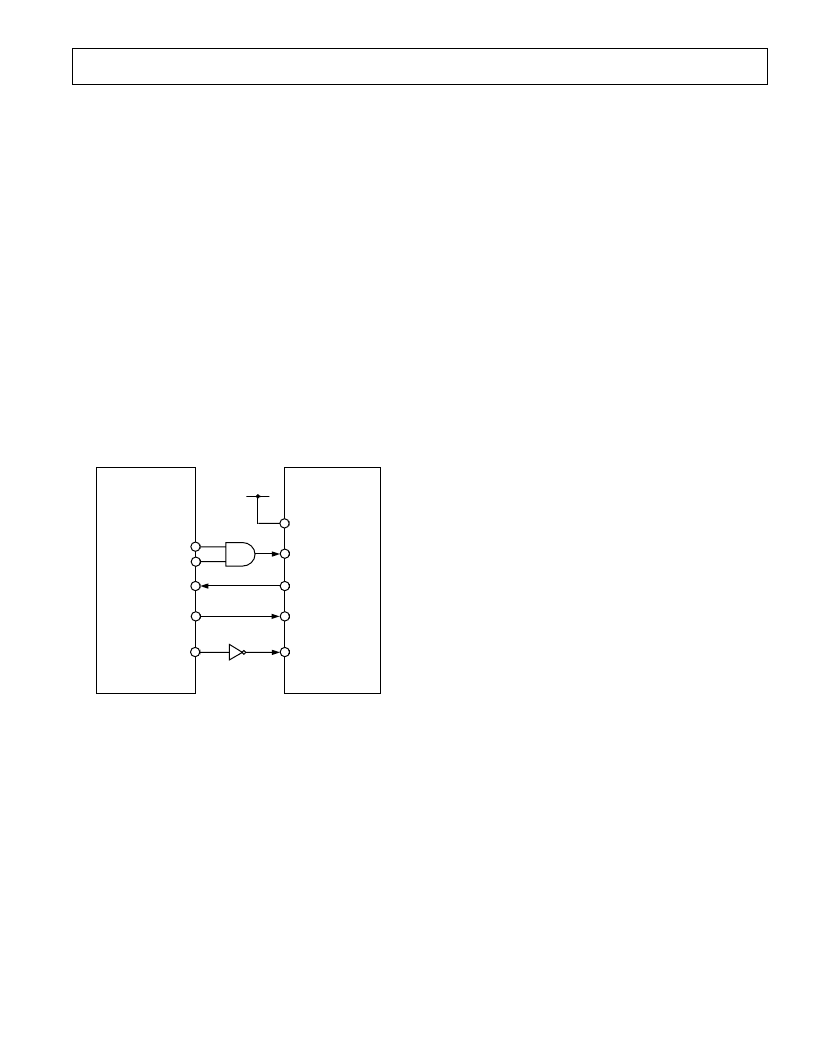
RFS
DT
ADSP-2103/
ADSP-2105
RESET
SCLK
DATA OUT
DATA IN
CS
AD7705/AD7706
V
DD
TFS
DR
SCLK
Figure 21. AD7705/AD7706 to ADSP-2103/ADSP-2105
Interface
AD7705/AD7706 to ADSP-2103/ADSP-2105 Interface
Figure 21 shows an interface between the AD7705/AD7706 and
the ADSP-2103/ADSP-2105 DSP processor. In the interface
shown, the
DRDY
bit of the Communications Register is again
monitored to determine when the Data Register is updated. The
alternative scheme is to use an interrupt-driven system, in which
case the
DRDY
output is connected to the IRQ2 input of the
ADSP-2103/ADSP-2105. The serial interface of the ADSP-
2103/ADSP-2105 is set up for alternate framing mode. The
RFS
and
TFS
pins of the ADSP-2103/ADSP-2105 are config-
ured as active low outputs and the ADSP-2103/ADSP-2105
serial clock line, SCLK, is also configured as an output. The
CS
for the AD7705/AD7706 is active when either the
RFS
or
TFS
outputs from the ADSP-2103/ADSP-2105 are active. The serial
clock rate on the ADSP-2103/ADSP-2105 should be limited to
3MHz to ensure correct operation with the AD7705/AD7706.
CODE FOR SETTING UP THE AD7705/AD7706
Table XVII gives a set of read and write routines in C code for
interfacing the 68HC11 microcontroller to the AD7705. The
sample program sets up the various registers on the AD7705
and reads 1000 samples from the part into the 68HC11. The
setup conditions on the part are exactly the same as those out-
lined for the flowchart of Figure 18. In the example code given
here, the
DRDY
output is polled to determine if a new valid
word is available in the data register. The very same sequence is
applicable for the AD7706.
The sequence of the events in this program are as follows:
1. Write to the Communications Register, selecting channel one
as the active channel and setting the next operation to be a
write to the clock register.
2. Write to Clock Register setting the CLK DIV bit which
divides the external clock internally by two. This assumes
that the external crystal is 4.9512 MHz. The update rate is
selected to be 50 Hz.
3. Write to Communication Register selecting Channel 1 as the
active channel and setting the next operation to be a write to
the Setup Register.
4. Write to the Setup Register, setting the gain to 1, setting
bipolar mode, buffer off, clearing the filter synchronization
and initiating a self-calibration.
5. Poll the
DRDY
output.
6. Read the data from the Data Register.
7. Loop around doing Steps 5 and 6 until the specified number
of samples have been taken from the selected channel.
相關PDF資料 |
PDF描述 |
|---|---|
| AD7706(中文) | 3 V/5 V, 1 Mw 2-/3-Channel 16-Bit, Sigma-Delta ADCs(三輸入通道16位A/D轉換器) |
| AD7705(中文) | 3 V/5 V, 1 Mw 2-/3-Channel 16-Bit, Sigma-Delta ADCs(完全差分輸入通道16位A/D轉換器) |
| AD7707BR | 3 V/5 V, +-10 V Input Range, 1 mW 3-Channel 16-Bit, Sigma-Delta ADC |
| AD7707BRU | 3 V/5 V, +-10 V Input Range, 1 mW 3-Channel 16-Bit, Sigma-Delta ADC |
| AD7707 | ECONOLINE: REC2.2-S_DR/H1 - 2.2W DIP Package- 1kVDC Isolation- Regulated Output- UL94V-0 Package Material- Continuous Short Circiut Protection- Internal SMD design- 100% Burned In- Efficiency to 75% |
相關代理商/技術參數 |
參數描述 |
|---|---|
| AD7707 | 制造商:AD 制造商全稱:Analog Devices 功能描述:3 V/5 V, +-10 V Input Range, 1 mW 3-Channel 16-Bit, Sigma-Delta ADC |
| AD7707BR | 功能描述:IC ADC 16BIT 3CH 20-SOIC RoHS:否 類別:集成電路 (IC) >> 數據采集 - 模數轉換器 系列:- 標準包裝:1,000 系列:- 位數:12 采樣率(每秒):300k 數據接口:并聯 轉換器數目:1 功率耗散(最大):75mW 電壓電源:單電源 工作溫度:0°C ~ 70°C 安裝類型:表面貼裝 封裝/外殼:24-SOIC(0.295",7.50mm 寬) 供應商設備封裝:24-SOIC 包裝:帶卷 (TR) 輸入數目和類型:1 個單端,單極;1 個單端,雙極 |
| AD7707BR-REEL | 制造商:Analog Devices 功能描述:ADC Single Delta-Sigma 500sps 16-bit Serial 20-Pin SOIC W T/R 制造商:Analog Devices 功能描述:ADC SGL DELTA-SIGMA 0.5KSPS 16BIT SERL 20SOIC W - Tape and Reel |
| AD7707BR-REEL7 | 制造商:Analog Devices 功能描述:ADC Single Delta-Sigma 500sps 16-bit Serial 20-Pin SOIC W T/R 制造商:Analog Devices 功能描述:ADC SGL DELTA-SIGMA 0.5KSPS 16BIT SERL 20SOIC W - Tape and Reel |
| AD7707BRU | 功能描述:IC ADC 16BIT 3CH 20-TSSOP RoHS:否 類別:集成電路 (IC) >> 數據采集 - 模數轉換器 系列:- 標準包裝:1,000 系列:- 位數:12 采樣率(每秒):300k 數據接口:并聯 轉換器數目:1 功率耗散(最大):75mW 電壓電源:單電源 工作溫度:0°C ~ 70°C 安裝類型:表面貼裝 封裝/外殼:24-SOIC(0.295",7.50mm 寬) 供應商設備封裝:24-SOIC 包裝:帶卷 (TR) 輸入數目和類型:1 個單端,單極;1 個單端,雙極 |
發布緊急采購,3分鐘左右您將得到回復。